
Professional PCB manufacturing and assembly
Building 6, Zone 3, Yuekang Road,Bao'an District, Shenzhen, China
+86-13410863085Mon.-Sat.08:00-20:00


BGA solder joint defects and related acceptance criteria
l Select the appropriate X-ray detection system
It is a very important task to choose an X-ray inspection system with high performance and price ratio suitable for actual production applications to meet the needs of quality control. Recently, the newer ultra-high resolution X-ray system has reached the micron level in detecting and analyzing defects, providing a more comprehensive and time-saving solution for finding hidden quality problems (including welding defects) on the production line. Before deciding to purchase an inspection X-ray system, be sure to understand the minimum resolution required by the system (see Table 8), and at the same time determine the approximate price of the system to be purchased. (Void detection resolution is generally 1/10 of the ball diameter)
Table 8 Applications of X-ray systems with different resolving power
Several aspects of system application
The minimum resolution required by the system
overall defect inspection
50um
General PCB inspection and quality control BGA inspection
10um
Fine Pitch Leads and Solder Joint Inspection
5um
uBGA detection
Flip Chip Inspection
PCB defect analysis and process control
Bond Crack Detection
1um
Microcircuit Defect Inspection
4. BGA solder joint defects and related acceptance criteria
Typical BGA defects are bridging, open circuits, missing solder balls, insufficient solder, large voids, displacement, large solder balls, and blurred edges of solder joints. 12.2.12 of IPC-A-610C specifically defines the acceptance criteria for BGA solder joints: smooth solder joints, clear boundaries, consistent diameter, volume, grayscale, and contrast of all solder joints, aligned positions, no offset or Twist, no solder balls and no voids etc. In practice, the standard can be appropriately relaxed, such as allowing the BGA solder joint to have an offset of no more than 25% relative to the solder pad, and the solder ball cannot be greater than 25% of the distance between the two nearest adjacent solder balls.
BGA solder joint void is a common defect. Its existence is prone to stress concentration and affects the reliability of solder joints. However, the presence of voids reduces the mechanical stress on the solder balls by reducing the space occupied by the solder balls. Voids generally appear in three layers: component layer, pad layer, and solder layer. Voids may exist in BGA solder balls before soldering, or they may appear after soldering. Air voids can occur due to the presence of vias in the solder paste material or on the surface of the pad or in the vicinity of the pad during board design. Small-sized voids are allowed inside the solder ball. IPC-7095 stipulates that the void area of the pad layer cannot be greater than 10% of the solder ball area, that is, the void diameter cannot exceed 30% of the solder ball diameter; the solder layer (the void is located on the solder ball) The void area in the middle) cannot be greater than 25% of the solder ball area, that is, the void diameter cannot exceed 50% of the solder ball diameter. The ratio of the void area to the solder ball area can be calculated as follows: if the void diameter is 50% of the solder ball diameter, then the void area is 25% of the solder ball area.
Deflection of the PCA due to stress from normal environmental use can cause cracking of a solder joint with voids towards the outside of the pad/ball connection or large voids. Voids greater than 35% of the BGA diameter or outside of solder joints found by X-ray inspection should be considered unacceptable.
If the void is completely encapsulated, cracking of the solder joint is unlikely because the stress will generally be applied uniformly to the pad/ball joint. Regardless, voids greater than 35% of the ball diameter indicate a process-related problem and should not be accepted.
hollow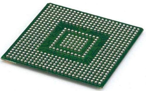
Solder voiding is caused by the expansion of compounds trapped in the solder during heating. Although voided BGA solder joints may indicate process issues that will cause future failures. Acceptable criteria in the solder joint should not exceed 20% of the solder ball diameter without a single void appearing on the outside of the solder joint. Multiple voids may appear in a solder joint, assuming the sum of the voids does not exceed 20% of the solder ball diameter.Desoldering solder joints
Desoldering of solder joints is not permitted.
Tin bridges and shorts
Bridging and shorting often occur when too much solder is at the contact point or when the solder is placed improperly. In the accepted standard, there cannot be shorted or bridged solder joints unless they are specifically designed into the underlying circuit or BGA.
Out of alignment
The X-ray image will clearly show if the BGA balls are not properly aligned with the pads on the PCB. Misalignment is not allowed.
Open circuits and cold solder joints
Open circuits and cold solder joints occur when the solder and corresponding pads do not make contact or when the solder does not flow properly. This is not allowed.
not in contact
Lost or misplaced solder and solder balls are not tolerated once components have been placed on the PCB.
X-ray evaluation
PCAs containing BGAs must be evaluated using an X-ray system capable of resolving holes at least less than 100 microns in diameter. The X-ray system must be able to allow the unit under test (UUT, unit under test) to be observed from top to bottom and obliquely.
The use of real-time X-ray inspection to evaluate solder joints and ensure a high process yield has become an essential element of successful BGA assembly. For these leadless assemblies, X-rays provide practical approval for successful soldering runs and reliable solder joints.
If the production run is well-coordinated, using a modern reflow oven, the self-aligning nature of the BGA makes x-ray inspection less likely to reveal too many defects. If so, the process should be checked immediately to determine if and where parameter limits have been exceeded.
1 Open circuit of non-removable BGA solder joints
Open circuits that occur at non-removable BGA solder joints are usually caused by contamination of the pads. Since the solder does not wet the pads on the printed circuit board, it "climbs" up the solder balls to the component interface. As mentioned above, the electronic test can confirm the existence of the open circuit, but it cannot distinguish whether it is caused by the pollution of the pad? Or is it caused by uncontrollable solder missing printing process? Testing with X-ray equipment also fails to reveal the open circuit due to the "shadow" of the front solder ball. Using cross-sectional X-ray inspection techniques, it is possible to discern such open circuits due to contamination through image slices taken between the pad layer and the component layer. Due to the open circuit phenomenon caused by pollution, there will be a small pad radius and a large component radius size, so the difference between the component radius and the pad radius can be used to distinguish whether the open circuit phenomenon is caused by pollution. The difference between the radii of open circuits due to insufficient solder is so small that it can only be discerned with cross-sectional x-ray inspection equipment.2 Void in detachable BGA soldering
Voids in detachable BGA soldering are caused by flowing vapor being trapped in the eutectic solder joint. Voids at removable BGA solder joints are a major defect phenomenon. During reflow soldering, because the buoyancy effect generated by the void is concentrated on the interface of components, most of the solder joint failures involved also occur there.
The occurrence of voids can be eliminated by preheating during the reflow process and by increasing the short preheat time and lower preheat temperature. When the void exceeds a certain size, quantity, or density, the reliability will be significantly reduced. However, there is also a saying that it is not necessary to limit the void, but to accelerate its cracking and diffusion, so that it will fail early and be eliminated. Voids in detachable BGA soldering can be clearly visualized in cross-sectional x-ray image slices acquired at the component layer. Some voids can be identified and measured within these images, or are manifested indirectly by a significant increase in the radius of the left DGA weld.


Just upload Gerber files, BOM files and design files, and the KINGFORD team will provide a complete quotation within 24h.