
Professional PCB manufacturing and assembly
Building 6, Zone 3, Yuekang Road,Bao'an District, Shenzhen, China
+86-13410863085Mon.-Sat.08:00-20:00

PCB design company detailed PCB design complete process
kinhford Electronics specializes in layout design for electronic products and can undertake multi-layer, high density PCB design panel business. With an average of more than 10 years of work experience in PCB design team, skilled use of market mainstream PCB design software, professional and efficient communication to ensure the progress of PCB design. Next, we will introduce the complete process of PCB design in detail.
1. Preliminary preparation
Preliminary preparation includes the preparation of component library and schematic diagram. Before the PCB design, the schematic SCH component library and PCB component packaging library should be prepared first.
The PCB component package library should preferably be built by the engineer based on the standard dimension data of the selected component. In principle, first build PC component packaging library, and then build schematic SCH component library.
PCB component package library has high requirements, which directly affects the installation of PCB. Schematic SCH component library requirements are relatively loose, but care should be taken to define pin attributes and correspondence with PCB component packaging library.
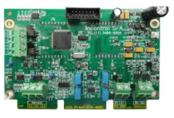
2. PCB structure design
According to the determined size of the circuit board and various mechanical positioning, PCB board frame is drawn in the PCB design environment, and the required connectors, keys/switches, screw holes, assembly holes and so on are placed according to the positioning requirements.
Fully consider and determine wiring and non-wiring areas (e.g., how much of the area around screw holes is non-wiring).
3. PCB layout design
Layout design is to place components in the PCB board frame according to the design requirements. Generate the network table (Design→Create Netlist) in the schematic tool, and then Import the network table (Design→ import Netlist) in the PCB software. After the network table is successfully imported, it will exist in the software background. All the devices can be called out by the Placement operation, and there is a flying line between the pins. Then the device layout design can be carried out.
PCB layout design is the first important process in the whole PCB design process. The more complex PCB board is, the better or worse the layout will directly affect the difficulty of the realization of the wiring later.
The layout design depends on the circuit foundation and design experience of circuit board designers, which is a higher level of requirements for circuit board designers. Junior circuit board designers are inexperienced, suitable for small module layout design or PCB layout design task with low difficulty of whole board.
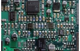
4. PCB routing design
PCB routing design is the most workload process in the whole PCB design, which directly affects the performance of PCB board.
In the design process of PCB, wiring generally has three levels:
The first is the cloth, which is the most basic entry requirements of PCB design;
The second is to meet the electrical performance, which is to measure whether a PCB board qualified standard, after the line layout, carefully adjust the wiring, so that it can achieve the best electrical performance;
Again is neat and beautiful, disorderly wiring, even if the electrical performance clearance will also bring great inconvenience to the later board optimization and testing and maintenance, wiring requirements neat and uniform, can not criss-cross without rules.
5. Wiring optimization and silk-screen placement
"PCB design is not the best, only better", "PCB design is a defective art", mainly because PCB design to achieve all aspects of hardware design requirements, and individual requirements may be conflicting, you can not have your cake and eat it.
For example, a PCB design project needs to be designed as a 6-layer board after evaluation by the circuit board designer, but the product hardware needs to be designed as a 4-layer board due to cost consideration, so the signal shielding layer can only be sacrificed, which leads to the increase of signal crosstalk between adjacent wiring layers and the decrease of signal quality.
A general rule of thumb for design is to optimize the wiring twice as long as the initial wiring. After PCB routing optimization is complete, post-processing is required. The main processing is the silk screen logo on the PCB board surface. During the design, the characters in the bottom layer of the silk screen must be mirrored to avoid confusion with the top layer of the silk screen.
6. ") https://www.kingfordpcb.com/yuan.php
https://www.kingfordpcb.com/yuan.php
Schematic diagram and structural element diagram are the most basic design requirements. Network DRC inspection and structural inspection are to confirm that PCB design meets the two input conditions of schematic diagram netlist and structural element diagram respectively.
Generally, circuit board designers have their own accumulated design quality Checklist, in which some items are based on company or department specifications and some are based on their own experience. Special inspection includes design Valor inspection and DFM inspection. These two parts focus on PCB design output back-end processing light drawing files.
7, PCB board
Before the PCB is formally processed into the board, the circuit board designer needs to communicate with the PE of the PCB plate supplier factory to reply the manufacturer's confirmation questions about PCB board processing.
Including but not limited to: PCB board type selection, line width and line distance adjustment, impedance control adjustment, PCB laminated thickness adjustment, surface treatment processing technology, aperture tolerance control and delivery standards.
How to choose PCBA patch manufacturer?
May 31,2023


Just upload Gerber files, BOM files and design files, and the KINGFORD team will provide a complete quotation within 24h.