Embedded component plate requirements
Embedded component printed circuit board (EDPCB) is a kind of product to realize high density electronic interconnection. Embedded component technology has great potential in PCB. Embedded element technology has the forming element buried method, printed element buried method, printed element is divided into thick film element and thin film element. The production of thin film components need special substrate, such as copper foil covered with nickel phosphorus alloy foil, for the production of thin film resistance; A high dielectric constant substrate is sandwiched between two sided copper-clad plates to make planar capacitors, forming a printed board with embedded passive components. There is also the development of polymer composite materials filled with ceramic powder, with high dielectric constant, low dielectric loss at high frequency, thin dielectric layer thickness, can be produced PCB inner layer RF capacitor. Embedded components are extended to flexible printed boards, and polyimide copper clad panels are also considered for making polyimide copper clad panels for film components.
Other special needs
Now there is Laser Direct Structuring (LDS) technology developed for the manufacture of model interconnecting devices for electronic circuits and component integration. The LDS process uses thermoplastic and metal oxide materials, formed by laser and metallized circuits. 3D printing technology is trying to be used in PCB manufacturing. Circuit graphics are not limited to two-dimensional planes, but become three-dimensional components. This technology also needs thermoplastic polymer materials.

Emerging medical electronic devices, some of which are implanted in the body, such as blood glucose transduction, diagnostic catheters, and cochlear implants, are based on bioinert substrates (PI or LCP) and stable pure precious metals (gold, platinum) as their conductors. The Internet of Things, smart home, smart city proposed, will be the new growth point of electronic information industry, will be equipped with a lot of new electronic equipment, there will be a lot of new PCB and its substrate demand, need to be prepared early, in time to join.
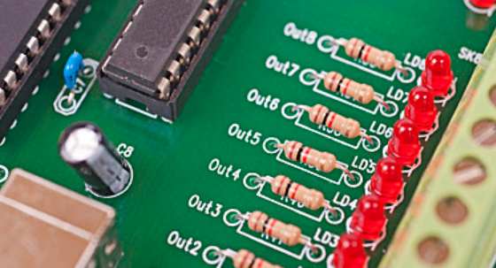
Printed circuit board (PCB) is an information carrier integrating various electronic components, which has a wide range of applications in the field of electronics. Its quality directly affects the performance of products. In the process of PCB manufacturing,PCB components are generally installed by surface patch installation technology. With the development of electronic technology and electronic manufacturing, electronic products tend to be lighter, smaller and thinner.
As an important part of modern electronic equipment, PCB board is required to further improve the integration degree of PCB board due to the small size of patch components and high installation density. In order to ensure the performance of electronic products, PCB board defect detection technology has become a very key technology in the electronic industry.
Circuit board defect detection includes two parts: solder spot defect detection and component detection. The traditional detection adopts manual detection method, which is easy to miss detection, slow detection speed, long detection time and high cost, and has gradually failed to meet the needs of production. Therefore, it is of great practical significance to design an efficient and accurate machine vision circuit board detection system equipped with industrial cameras instead of human eyes.
Machine vision detection technology is built on the basis of image processing algorithm, through digital image processing and pattern recognition method to achieve, compared with the traditional manual detection technology, improve the efficiency and accuracy of defect detection.
Machine vision system generally adopts CCD or CMOS industrial cameras to capture detection images and convert them into digital signals, and then processes the image digital signals through computer software and hardware technology, so as to obtain the required feature values of various target images, and thus achieve parts recognition or defect detection and other functions. With many years of experience in visual inspection, we provide professional system configuration schemes and image acquisition products according to customers' different requirements for circuit board inspection.


