
Professional PCB manufacturing and assembly
Building 6, Zone 3, Yuekang Road,Bao'an District, Shenzhen, China
+86-13410863085Mon.-Sat.08:00-20:00

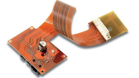
Application range of flexible printed boards
pcba manufacturers commonly used flexible printed boards in a wide range of applications, almost in all kinds of electronic products can be used, its application scope has a trend of exceeding rigid printed boards.
The flexible PCB wiring used for making pcba proofing is more complex, and flexible circuit is a more ideal design choice when multi-signal processing or special electrical and mechanical properties are required. Flexible assembly is most economical when the size and performance used exceed the capability of rigid printed circuits. Flexible circuits use films that are protective and cure at higher temperatures, have higher glass transition temperatures, and are superior to rigid printed boards in terms of lead-free and halogen-free.
Although the cost of substrate used in pcba production factory is relatively high, with the development of new materials for pcba patch and the increase of production, the price of flexible plate gradually decreases. The new material changes the substrate structure and improves the production process. The new structure makes the thermal stability of the product higher and the material match better. Newer materials allow more sophisticated wires to be made from thinner layers of copper, and IC carriers can be used to make packages lighter and better fit in smaller Spaces. The new technology of these materials can produce copper layers several microns thick and obtain fine wires with 3mil or even narrower widths, which makes the manufacturing and cost performance of flexible printed boards close to that of rigid printed boards, thus making the application of pcba patches more and more wide.
2. Structure and manufacturing process of Type I HDI board
(1) The structure of type I HDI board
The middle of pcba manufacturer's board is prefabricated core board, the outermost layer is semi-cured sheet and RCC pressed insulation layer, and then through drilling, hole metalization, outer pattern transfer, plating, etching and other processing into a first-order blind hole and through hole HDI board. If second-order blind hole is needed, then the second-order blind hole HDI plate can be obtained by adding semi-cured sheet and RCC secondary lamination on this basis, and repeating the steps of drilling, hole metallization, pattern transfer, plating, etching, etc.

(2) Manufacturing process of type I HDI board
The manufacturing process of type I HDI board can be divided into two types according to the way of drilling.
Process 1: Using resin-attached copper foil (RCC) and semi-cured sheet laminated, drilling directly with UV-CO2 laser.
Core plate fabrication → inspection → surface treatment → superimposed semi-curable sheet and RCC→ pressing → Positioning, laser drilling → hole metallization → pattern transfer → development → electroplating → removal of protective film → etching →AOI inspection → coating protective film selective plating → contour processing → electrical measurement → final inspection → packaging
Process 2: Drilling with CO2 laser using RCC and chemical etching window.
Core plate fabrication → inspection → surface treatment → superimposed semi-curable sheet and RCC→ pressing → positioning of the pattern of the hole → etching the window of the hole →CO2 laser drilling → removal of protective film → metallization of the hole → pattern transfer → development → electroplating → removal of protective film → etching → AOI inspection → coating protective film selective plating → shape processing → electrical measurement → final inspection → packaging
2. The structure and manufacturing process of Type II HDI board
(1) Structure of Type II HDI board
The basic structure of Type II HDI board is shown in the figure. The middle of the board is a prefabricated core board. The through hole on the core board is filled with resin, and after grinding and leveling, the outermost layer is added with semi-cured sheet and RCC pressed insulation layer, and then the HDI board with first-order blind hole, buried hole and through hole is made by drilling, hole metalization, outer pattern transfer, plating, etching and other processing. If second-order blind hole is needed, then the second-order blind hole HDI plate can be obtained by adding semi-cured sheet and RCC secondary lamination on this basis, and repeating the steps of drilling, hole metallization, pattern transfer, plating, etching, etc.
(2) Manufacturing process of Type II HDI board
The manufacturing process of Type II HDI board can be divided into two types according to the way of drilling.
Process 1: Drilling directly with UV-CO2 laser using RCC and semi-cured sheet laminated.
Core plate fabrication → inspection → resin filling through hole → grinding → surface treatment → superimposed semi-curable sheet and RCC→ pressing → Positioning and laser drilling → hole metallization → pattern transfer → developing → electroplating → removal of protective film → etching →AOI inspection → coating protective film selective plating → contour processing → electrical measurement → final inspection → packaging
Process 2: Chemically etched window and drilled with CO2 laser.
Core plate fabrication → inspection → resin filling through hole → grinding → surface treatment → superposition semi-curable sheet and RCC→ pressing → Positioning of the pattern of the fabrication hole → etching hole window →CO2 laser drilling → removal of protective film → metallization of hole → pattern transfer → development → electroplating → removal of protective film → etching →AOI inspection → coating protective film selective plating → shape processing → electrical measurement → final inspection → packing
The above two processes are typical processes used in pcba manufacturing. In addition, pcba processing can also be done without resin copper foil. After layer upon layer of semi-cured sheet or photosensitive resin on the core plate, the drilling mask can be made directly on the cured semi-cured sheet or exposed photosensitive resin by CO2 laser drilling. Then, the semi-addition process is adopted to coarse-surface for chemical copper deposition and copper plating. When the thickness of the copper layer meets the requirements, the graphic transfer and etching are carried out. In short, the same kind of HDI board, according to the use of different laminated materials or different ways of pore-forming, the production process of pcba is different, must be flexibly selected according to the substrate materials used in pcba patches and production equipment conditions.
Through hole weldability test
May 26,2023


Just upload Gerber files, BOM files and design files, and the KINGFORD team will provide a complete quotation within 24h.