
Professional PCB manufacturing and assembly
Building 6, Zone 3, Yuekang Road,Bao'an District, Shenzhen, China
+86-13410863085Mon.-Sat.08:00-20:00

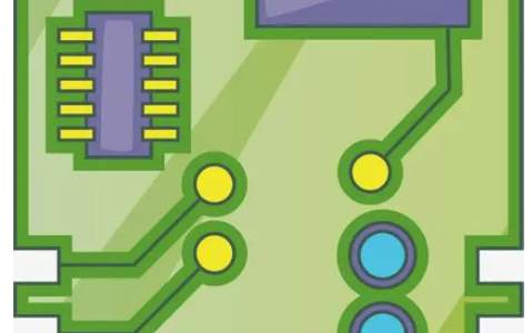
PCB circuit boardis an insulating board as the base material, cut into a certain size, it is attached with at least one conductive graphic, and cloth holes (such as component holes, fastening holes, metallization holes, etc.), used to replace the chassis of the previous device electronic components, and realize the mutual connection between electronic components. Nowadays, PCB circuit board develops from single layer to double panel, multilayer board and flexible board, and continuously develops to the direction of high precision, high density and high reliability, and the application is more and more widely.
First, seasonal maintenance:
1. Clean the dust on the PCB circuit board every quarter. Use the special cleaning solution for the circuit board to clean the dust.
2. Observe that the electronic components in the circuit have no traces of high temperature, and the electrolytic capacitor has no leakage phenomenon, if any, it should be replaced.
Two, annual maintenance knowledge:
1. Clean the dust on the pcb board.
2. Spot check the capacity of electrolytic capacitors in pcb circuit boards. If it is found that the capacity of electrolytic capacitors is less than 20% of the nominal capacity, it should be replaced.
3. If the high-power components are coated with heat dissipation grease, check whether the heat dissipation grease is dried. If the heat dissipation grease is dry, remove the heat dissipation grease and apply new heat dissipation grease to prevent the high-power components of the circuit board from burning out due to poor heat dissipation.
Attention should be paid to Pcb circuit board production

With the rise of the electronic industry, circuit board production and development has become a more and more important part of PCB proofing a circuit board is not simple, easy to say. So, in the production of circuit board development and production need to pay attention to what? Shenzhen Lianxinghua pcb circuit board manufacturer respectively from the design of circuit board and circuit board production of these two aspects to explain
First, the design of circuit board need to pay attention to what aspects
1) Single side pad:
Do not use filler blocks to act as surface mount elements of the pad should be single sided pad Normally single sided pads are not drilled, so the aperture should be set to 0
2) Do not use welding pad instead of hole, and vice versa.3) character annotation should try to avoid the welding pad,
4) Welding green oil requirements:
A. In general, according to the specification design, the welding points of the components are represented by a pad, which will automatically not solder.
B. In addition to the solder plate on the circuit board, if certain areas need to be free of solder resistance ink, it should be expressed with solid graphics on the corresponding layer.
C. The through hole pad beside the bga pad shall be covered with green oil on the component surface.
5) Copper area requirements: Whether it is made of grid or solid copper, the distance from the plate edge is greater than 0.5mm. The size of copper-free grid points must be larger than 15mil x 15mil.
6) Contour machining drawings should be drawn at Mech1 layer
7) The hole diameter of the pad should be set as the width of the long hole, and the outline of the long hole should be drawn on the Mech1 layer.
8) When placing components at the early stage of the general wiring, the foot diameter, pad diameter, hole aperture and hole disk diameter should be considered, so as to avoid the inconvenience caused by the wiring and then modification.
Two, pcb circuit board production problems need to pay attention to:
1) Circuit analysis, and in order to smooth the signal circuit is divided into basic units?
2) Where it is necessary to screen, is it being effectively screened? 3) Whether basic grid graphics are used
4) Whether the size of the printed board is the optimal size 5) whether the selected wire width and spacing are used as much as possible
6) Whether the preferred pad size and hole size are used. 7) Whether the photographic plate and schematic drawing are appropriate
9) The letters should be visible after assembly, pay attention to the size and model
10) Whether a large area of copper foil opens a window
11) The production of modern circuit boards involves chemical, electronic, computer, machinery and printing and other technical equipment.
The production process is long and complex. A typical PCB factory's production process is as follows:
1, blanking →2, inner layer production →3, pressing →4, drilling →5, copper plating →6, outer layer production →7, welding resistant paint printing →8, text printing →9, surface treatment →10, shape processing.


Just upload Gerber files, BOM files and design files, and the KINGFORD team will provide a complete quotation within 24h.