
Professional PCB manufacturing and assembly
Building 6, Zone 3, Yuekang Road,Bao'an District, Shenzhen, China
+86-13410863085Mon.-Sat.08:00-20:00

PCB circuit board designshould take into account its beauty, when the circuit board turns the line to have a form of bad choice, the design needs to set the circuit board PCB circuit board corner routing form corner mode. You can choose 45°, 90°, or arc. Generally do not use sharp corners, it is best to use arc transition or 45° transition, avoid using 90° or more sharp corner transition.
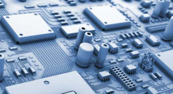
Whether it is PCB circuit board or aluminum base circuit board or single sided circuit board, they all have a common name, that is circuit board or circuit board. These circuit boards in the design of our heart to treat, PCB circuit board wire through the two pads and not connected to the time, should maintain the maximum and equal spacing with them, the same wire and wire of the wire through the two pads and not connected to the time, should maintain the maximum and equal spacing with them, The spacing between them should also be equal and maximum. The spacing between them should also be equal and maximum. The connection between the wire and the pad should also be as smooth as possible to avoid small pointy feet, which can be solved by the method of filling tears. When the center distance between pads is less than the outer diameter D of a pad, the width of the wire can be the same as the diameter of the pad; If the center distance between pads is greater than D, the width of the wire should not be greater than the diameter of the pads.

The difference between through - hole plug-in technology and surface mounting technology in SMT patch processing
The characteristics of SMT technology can be compared with traditional through-hole insert technology (THT). From the perspective of assembly technology, the fundamental difference between SMT and THT is "paste" and "insert". The differences between the two are also reflected in the substrate, components, component forms, solder joint forms and assembly process methods.
The welding process of the old version of THT plug-in adopts leaded components. The circuit connecting wires and mounting holes are designed on the printed board. After inserting the leaded components into the pre-drilled through holes on the PCB, the components are temporarily fixed and welded on the other side of the substrate with soft brazing technology such as wave soldering to form reliable solder joints and establish long-term mechanical and electrical connections. The main parts and solder joints are distributed on both sides of the substrate. Using this method, because the components have leads, when the circuit density to a certain extent, it can not be solved to reduce the size of the problem. At the same time, it is difficult to eliminate the faults caused by the proximity of the leads and the interference caused by the length of the leads.
DIP packaging (DualIn-linePackage) is a kind of part packaging in THT plug-in technology, also known as dual in-line packaging technology, which is one of the simplest packaging methods. It refers to an integrated circuit chip packaged in dual-in-line format. Most small and medium-sized integrated circuits are packaged in this format, and the number of pins usually does not exceed 100. The DIP-packaged CPU chip has two rows of pins that need to be plugged into the chip socket that has the DIP structure.
The so-called surface assembly technology refers to the assembly technology of electronic parts with certain functions by placing the components with flake structure or the miniaturized components suitable for surface assembly on the surface of the printed board in accordance with the requirements of the circuit and assembling them by welding processes such as reflow welding or wave soldering. The differences between SMT and THT components in mounting and welding are shown in the figure. On traditional THT printed circuit boards, the components and solder joints are located on two sides of the board; On the SMT circuit board, solder joints and components are on the same surface of the board. Therefore, on SMT printed boards, through holes are used only to connect the wires on both sides of the board, the number of holes is much smaller, and the diameter of the holes is much smaller. In this way, the assembly density of the circuit board can be greatly improved.
Shenzhen Hongyunlai Electronic Technology Co., LTD., to give you the best quality SMT patch processing,PCB production, embedded system research and development, electronic processing, embedded motherboard,PCBA contract materials, Guangzhou PCBA processing services.


Just upload Gerber files, BOM files and design files, and the KINGFORD team will provide a complete quotation within 24h.