
Professional PCB manufacturing and assembly
Building 6, Zone 3, Yuekang Road,Bao'an District, Shenzhen, China
+86-13410863085Mon.-Sat.08:00-20:00

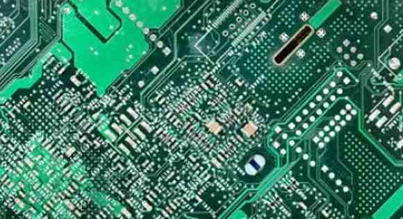
The main reasons for PCB board bursting or Delamination are the following two categories: a board absorbing diα2 /z-CTE is too big, and the bursting caused by "board absorbing water" accounts for 70% of the defects. Other reasons include PCB structure's uneven growth and contraction. Cold and heat imbalance, process injury and bad blackening... Although we can not rule out the possibility, but the ratio is not too high.
Why "water" is the main cause of PCB board burst?
The "water" has little effect on the bursting plate below 100°C.
When the temperature exceeds 100°C, the "water" becomes the resin's plasticizer.
If the resin absorbs more water, Tg will decrease (△Tg should be less than 5°C), and the rubber state will come earlier, it will cause instant Swelling (Swelling) in the Z direction of the plate and rapid cracking (it is most likely to happen between 100°C and Tg). The pressure (psi) of water vapor increases in a geometric progression beyond 100°C.
Generally, the CTE(expansion coefficient) of X and Y plates is relatively stable, between 15 and 16ppm/°C. In addition, the hidden water in the plate will also become a plastic resin, and the outside of the water together to help.
When the resin temperature exceeds the Tg point, it will change into rubber state. At this time, the "water" part of the explosive plate has become a supporting role, and at this time, most of the water has been evaporated into steam. Moreover, the rubber state is soft, and it is not easy to have explosive plate.
Where does the PCB "water" come from?
Since the "water" is so important to the explosion plate, then we have to study where the water comes from, on our general understanding and cognition, most of the "water" may come from the outside world, may be inhaled in the PCB process attached, or PCB storage from the environment gradually Diffusion (Diffusion) into; But the internal structure of the plate is easy to hide water is also one of the possible reasons; The other thing you might not expect is that PCB resins have water molecules embedded in their formula, which, when heated, creates its own water. So in summary, the plate absorbs "water" and the water storage place is:
Analysis of the real cause of PCB board explosion and countermeasures
Water is the structure of resin molecules themselves (molecules of similar polarity already have water molecules in them, and whenever there is OH in the formula it will form).

Resin and glass fiber interface is easy to hide water (the board uses a resin and a glass fiber woven with warp and weft, if the weaving is not dense enough, there will be gaps, it is generally recommended to choose low permeability flat fiber cloth is not easy to hide water).
Resin and copper foil interface is also easy to hide water.
The holes in the plates will hold water.
PCB absorbent explosion board improvement program - baking
Since "water" is the main cause of PCB board burst, so as long as the water removal inside the PCB should be able to solve most of the problem of board burst, and [baking] is the best way to remove the PCB external water. Since the purpose of baking is to remove moisture, the baking conditions are best to meet the following requirements:
Heat the oven to a temperature just above 100°C (105°C is recommended, because the oven temperature can be inaccurate), so that the water can be turned into steam and can be easily dispersed.
When baking, it is best to separate each board, so that the moisture is more easily volatilized. If PCBS are stacked on top of each other, water will not escape effectively.
The oven must have an air vent, otherwise it is useless to bake the oven full of steam.
From the selection of PCB board and the process to control the water absorption conditions
Although baking is the best way to improve the burst board, baking not only wastes time, but also wastes equipment and manpower, and the Tg value will decrease after baking PCB is also a problem. A better method is to control the water absorption conditions from the selection of PCB board and the manufacturing process.
1. If the plate itself has polarity, it is easy to absorb water. Try to choose not absorbent resin to prevent the plate from absorbing water.
2. Open (flat) fiber cloth can be used. Reduce the gap between resin and glass fiber interface to reduce the possibility of easy water storage. (The following picture is only a schematic, not the real glass fiber cloth, basically by the warp and weft two strands of material staggered woven, if there is a gap between the warp and weft, it is easy to hide water, so generally to check the tightness of the tightness, the better the tightness, the smaller the breathability, the less easy to hide water, the high-frequency circuit board is also relatively no loss and signal equal one problem.)


Just upload Gerber files, BOM files and design files, and the KINGFORD team will provide a complete quotation within 24h.