
Professional PCB manufacturing and assembly
Building 6, Zone 3, Yuekang Road,Bao'an District, Shenzhen, China
+86-13410863085Mon.-Sat.08:00-20:00

The RF PCB and microwave pcb industries are growing rapidly, and the trends that drive faster and cheaper production of PCB assemblies continue. This aggressive pace has caused PCB design rules to clash with component requirements. The disconnect between designers and manufacturers leads to blind adherence to these rules, which eliminates the opportunity to improve performance.
These problems require designers to be aware of potential problems and pitfalls in order to avoid them. This guide discusses some of the challenges specific to RF and microwave circuit design and suggestions on how to address them, covering everything from basic design tips to practical advice for high-volume RF assembly.
Basic design guide for RF PCB and microwave PCB assembly
Here are some pitfalls in the process, designed to prevent them from happening.
Component placement
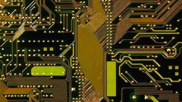
Components shall be placed as close to the center of the RF and microwave PCB board as possible. This minimizes parasitic inductors, which degrade performance at higher frequencies. Components should also be placed as close to their pairing connectors as possible. This reduces coupling between routes and improves signal integrity. For example, if you are designing a high-speed digital interface board, it is critical to keep the wires at a minimum distance from each other on opposite sides of the board. This minimizes crosstalk between signals on different layers on RF and microwave PCB boards.
Poorly grounded
Grounding is a key aspect of any circuit. If you have any poor grounding in your RF and microwave PCB designs, you could end up interfering with other circuits or even damaging your circuits. For example, if your RF and microwave PCB boards have traces on both sides, one side may have a better connection than the other (due to different environmental conditions). This can lead to problems. To avoid this, use multiple holes and thick tracks to ensure that all tracks are well grounded throughout their length.

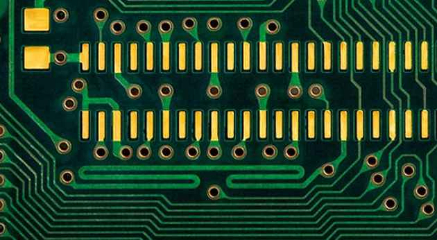
Routing optimization
The routing path can be optimized to reduce noise by eliminating holes (interconnect points) in unwanted areas. Through-holes are often used as ground connections to help reduce airborne radiation. However, if the throughholes are located near high impedance points on RF and microwave PCB boards, such as power lines, they can also be used as antennas. In this case, they may radiate electromagnetic energy into free space or other nearby conductors, such as traces or cables at the ground plane.
Cyclic region
The loop region results in signal deterioration due to its high impedance compared to linear routing. Therefore, whenever possible, use multiple pass holes rather than single pass holes to minimize loop area, or place them as close to the component pads as possible so that they have the minimum length of printed circuit board between them and the component pads that need to be connected to the pass holes in RF and microwave.
Conducted noise
Conductive noise travels through a conductive path, such as a trace or ground connection. Conducted noise may be caused by switching transistors, microcontrollers, or other electronic devices on RF and microwave PCB boards. When these devices are turned off, they emit spikes of current that create electromagnetic fields that radiate from your RF and microwave PCB boards. These spikes, called transient current spikes, can pass through the grounding layers on RF and microwave PCBS, and if they reach the antenna at the end of the board, they generate electrostatic discharge (ESD) events.
Use multilayer RF PCB and microwave PCB board
The more layers added to RF and microwave PCB boards, the greater the copper surface area available for heat dissipation and to provide a return path for current. This means that multilayers are well suited for high frequency applications such as RF/microwave systems, where heat dissipation must be efficient while maintaining a low impedance return path for high frequency current in the antenna.
Echo signal loss
Antenna return signal loss is an important consideration in RF and microwave PCB design. The return loss of any RF and microwave PCB board is defined as the power ratio between the forward and reflected waves at a given frequency. Ideally, the value should be greater than -20 dB at all frequencies of interest. In practice, however, you should consider -10 dB the minimum requirement for most applications.
Major contributors to return loss include impedance mismatch and leakage current in the grounding formation. Impedance mismatches between the antenna and its associated components can result in reflections, which can lead to reduced efficiency and performance. For example, ensuring that the impedance match between the antenna and the coaxial cable is within +/- 2% will help ensure good efficiency.
Leakage currents may also cause considerable loss by reflecting signals back to their source circuits or radiating them into free space, thereby interfering with other equipment or systems on RF and microwave PCB boards.
Characteristics of RF PCB laminates
May 11,2023


Just upload Gerber files, BOM files and design files, and the KINGFORD team will provide a complete quotation within 24h.