
Professional PCB manufacturing and assembly
Building 6, Zone 3, Yuekang Road,Bao'an District, Shenzhen, China
+86-13410863085Mon.-Sat.08:00-20:00

Decoupling capacitor is a passive electronic component. It reduces power supply noise by diverting the power supply to the ground or a lower voltage level. The main purpose of the decoupling capacitor is to filter the power supply and ensure that there are no fluctuations on the power line.
Since the decoupling capacitor has a large capacitance value, it acts as a low-pass filter and absorbs high frequency noise in the circuit. This reduces interference in the circuit and makes it more stable. The frequencies of high-speed signals can be very high, so you must ensure that your decoupling capacitor has enough capacitance to absorb these high frequencies.
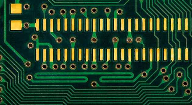
Use Via Stitching to form a solid ground plane
Through-hole stitching is the best way to connect two or more ground layers in high-speed or RF PCB designs. This technique uses small through-holes between the trace in one plane and the corresponding through-holes in the other plane, thus forming conductive Bridges between the planes. The result is a single connector that spans multiple layers, providing better RF performance than using a single connector.
When using through-hole stitching to create a single bonding layer, it is critical to use appropriate spacing for each through-hole so that the stitching does not result in electrical crosstalk between routes. In general, the spacing between the holes in adjacent tracks should be about ten times the diameter of the holes. The distance between the through-holes on different layers should be about five times the diameter of the through-holes.
Rotate parts to avoid 90 degree angles
When wiring high speed and RF PCBS, it is essential to avoid 90 degree angles. The copper wire is then connected at 90 degrees, and the signal will bounce back and forth between them. This interference results in signal attenuation, crosstalk between signals, and unwanted emission that interferes with other nearby circuits.
To avoid these RF PCB problems, you need to rotate the components so that they are not connected at right angles. The easiest way to do this is to rotate the pads on the assembly until they form an Angle of less than 90 degrees. For example, if a pad is 0.1 inches from a trace on one side and 0.2 inches from another trace on the other side, rotate the pad so that its center line is closer to the first trace than the second.

Maintain a symmetrical RF PCB layout as much as possible
One thing that helps in wiring high speed and RF PCB circuits is maintaining the symmetry of the layout. This helps minimize inductance between signals that may be located on adjacent layers.
For example, when an antenna orientation diagram is laid out on an RF PCB, it is advisable to keep the antenna elements symmetrical around the centerline of the board. This will help reduce noise and interference from surrounding wiring and components.
It is also important to keep the high-speed wiring symmetrical around the center line of the board. The high-speed signal will travel further on one side of the wire before moving to the center line of the board. This can lead to asymmetric reflections from nearby wiring, which can distort or degrade the signal.
Set up prohibited area
Forbidden areas or areas are predefined areas that should not be wired. Restricted areas are often used to avoid sensitive components, such as antennas, antenna switches, and connectors in RF PCB domains. The reserved area is the area where you want to wire the layout within a specified tolerance range. If the layout wiring is in a reserved area, it must meet specified tolerances and timing requirements.
Identify high speed network and adjust width
Identifying high-speed networks and adjusting their width accordingly is key to manufacturing high-speed and RF PCBS that minimize signal integrity issues.
High speed network identification
Identifying high-speed networks on boards is the first step in designing quality RF PCBS for high-speed or RF applications. These networks typically include wiring between two devices and from one end of the circuit board to the other.
You can identify these traces by looking at how they are wired in your RF PCB design. They should be routed in the inner layer, away from ground layers and other routes that may cause reflection of signal paths.
Adjust the width of RF PCB
Once you have identified your high speed networks, you should adjust their widths according to their impedance values to ensure the appropriate signal propagation speed within them. Impedance values depend on several factors, including line length and dielectric thickness, but in general; Impedance values are higher when the distance between two conductors is greater or when there are more gaps in the conductor material, such as copper.
Final judgment
There is no silver bullet for high-speed and RF PCB wiring, but following these best practices will help you jump-start your next RF PCB project and design boards that are less likely to generate unwanted electromagnetic interference. Having said that, it is important to understand that high-speed and RF PCB wiring is not much different from typical PCB wiring. It just needs more attention to detail. Visit Taofang Electronics for more information on high speed and RF PCBS.


Just upload Gerber files, BOM files and design files, and the KINGFORD team will provide a complete quotation within 24h.