
Professional PCB manufacturing and assembly
Building 6, Zone 3, Yuekang Road,Bao'an District, Shenzhen, China
+86-13410863085Mon.-Sat.08:00-20:00

13 basic rules for isobar PCB layout
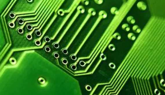
1. According to the layout of the circuit module, the related circuit with the same function is called a module. The components in the circuit module should adopt the principle of nearby concentration, and the digital circuit and the analog circuit should be separated at the same time.
2. Do not install electronic components, such as tooling holes and standard holes, within 1.27mm of non-mounting holes. Do not install components within the range of 3.5mm (M2.5) and 4mm (M3) around mounting holes such as screws.
3, horizontal installation of resistance, inductance (plug-in), electrolytic capacitor and other components below avoid drilling, so as to avoid the hole after wave soldering and component shell short circuit;
4. The distance between the outside of the component and the edge of the plate is 5mm;
5. The outside of the mounting element and the outside of the adjacent insert element are greater than 2mm;
6, metal shell components and metal parts (shielding box, etc.) should not contact other components, not close to the printed circuit, welding pad, spacing should be greater than 2mm. The other side of the positioning hole, fastener mounting hole, oval hole, and plate square hole is greater than 3mm.
7, the heating element can not be close to the wire and heat sensitive element; High heat element should be evenly distributed;
8. The power socket should be as close to the printed circuit board as possible. The power socket and the bus terminal connected to it should be placed on the same side. Special care should be taken not to place power sockets and other welded connectors between the connectors for easy connection. These sockets, connectors are welded and power cord designed and cable ties. The spacing between the power socket and the welded joint should be considered to facilitate the insertion and removal of the power plug.
9. Other components: All IC components? The polarity of the polar element is clearly marked. The polarity on the same printed board shall not exceed two directions. When there are two directions, they are perpendicular to each other;
10, the surface of the board should be properly dense, density difference is too large, should be filled with mesh copper foil, mesh greater than 8mil (or 0.2mm);
11, chip pad can not have? Through hole, avoid solder paste loss caused by loss of solder joint. Important signal cables are not allowed to pass through the socket pins;
12. The patch is aligned on one side, the character direction is consistent, and the packaging direction is consistent;
13. The polarization element should be as consistent as possible in the direction marked by polarity on the same plate.
Ii. Wiring rules for components
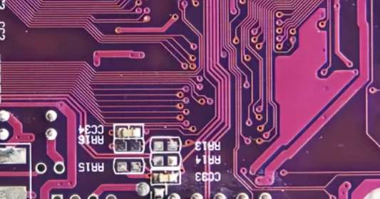
1. Wire in the area less than or equal to 1mm from the PCB board edge and within 1mm around the mounting hole.
2. The power cord should be as wide as possible, not less than 18mil; Signal line width shall not be less than 12mil; cpu input/output should not be less than 10mil (or 8mil); Line distance not less than 10mil;
3, the normal through hole is not less than 30mil;
4, double in-line insert: 60mil pad, 40mil aperture; 1/4W resistance: 51*55mil (0805 surface mount); PAD embedded 60mil, 42mil aperture; Unlimited capacitance: 51*55mil (0805? Surface mount); PAD wire 50mil, aperture 28mil;
5. As far as possible, the power cable and the ground should be radial, and the signal cable should not appear loopback.
Revolutionize PCB production

The method of printing PCBS has not changed for decades. In the early days of imaging circuit boards, the substrate (copper laminate) was screen-printed with liquid anti-corrosive agent; It is then cured in the oven.
This allows the resist to act as a mask during the subsequent etching process. The screen both applies the coating and creates the exact trajectory image required on the strip.
In the 60s and 70s, the demand for PCBS grew exponentially, and better ways to pack more components onto the board in less space, which led to the development of dual panels and multi-layer modules. The next step was to find a reliable way to attach the plate sides to the beginning, which involved soldering wire links, but eventually this was replaced by the more reliable "plated through hole" method, which is the common method of attaching one layer to another today.
Moisture resistance
In the 1970s and early 2000s, track density increased and circuits with more than 12 interconnect layers became commonplace. Track widths are getting smaller and smaller, up to 100 microns.
Traditionally, wet resist was used and is still used as a de facto printing method in industry. However, this method is not perfect and has many disadvantages.
Wet resist is usually inexpensive, but requires precuring before printing and tends to be used in mass production due to the capital cost of curing furnaces. Handling is also often problematic because wet resist cannot be touched. Partially cured resist also attract dust particles due to their sticky surface. For these reasons, many in the industry are turning to dry film methods.
Basically, dry film is a partially dried wet resist sandwiched between two layers of mylar. After coating, a layer of mylar is removed on a special laminator, then the partially dried resist (dry to the touch) is laminated onto the copper substrate under heat and pressure. Although dry film is more expensive than wet resist, convenient processing makes it a useful material forPCB imaging and etching.
How can SMT factory manage well
May 10,2023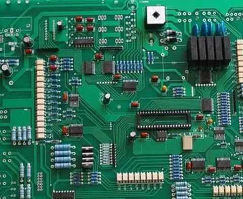


Just upload Gerber files, BOM files and design files, and the KINGFORD team will provide a complete quotation within 24h.