
Professional PCB manufacturing and assembly
Building 6, Zone 3, Yuekang Road,Bao'an District, Shenzhen, China
+86-13410863085Mon.-Sat.08:00-20:00

Circuit board can be called printed circuit board or printed board, FPC circuit board, FPC circuit board is also called flexible circuit board Flexible circuit board is made of polyimide or polyester film as a substrate with a high degree of reliability, brilliant flexible printed circuit board. Circuit board names are: porcelain ceramic circuit board, oxygen aluminum ceramic circuit board, aluminum nitride porcelain ceramic circuit board, circuit board, PCB board, aluminum substrate, high frequency board, thick copper board, impedance board, PCB, ultra-thin circuit board, ultra-thin circuit board, printing (copper etching technology) circuit board, etc.
1. Office principles
The office principle of the PCB circuit board is to use the board based insulation material isolation to the surface copper foil conductive layer, to obtain the current along the preset route in the various components of the flow to complete such as work, amplification, attenuation, modulation, demodulation, coding and other functions.
2. Composition
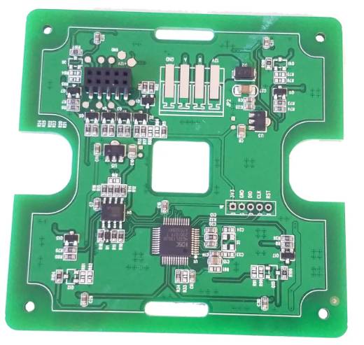
The circuit board is mainly composed of solder pad, through hole, mounting hole, wire, element and connector. The film circuit SMT of Waterford circuit board is composed of film circuit SMT, supplement, electrical boundary, etc. The main function of each component is described as follows:
Pad: Metal hole for burning the pin of a welding element.
Through holes: There are metal through holes and non-metal through holes, the metal through holes are used for connecting the components between each layer.
Mounting hole: used to secure the circuit board.
Conductor: Electrical network copper film used for pins of co-signer components.
Connector: A component used for linking circuit boards.
Add: Applied copper for ground wire network, can reduce the impedance of pipe.
Electrical boundary: Used to confirm the size of the circuit board. All components on the circuit board cannot exceed this boundary.
3. Sort
Circuit boards according to the number of layers to be divided into single panel, double panel, and multilayer circuit boards three big classification.
Multilayer board: a printed board consisting of three or more layers of conductive graphics and insulating materials between which the conductive graphics are interconnected as required. Multilayer circuit board is the product of electronic information technology to high speed, multi-function, large volume, small size, thin, lightweight direction.
Single panel: On the most basic PCB, the parts are concentrated on the inside side and the wires on the other side. This PCB is called a single-sided circuit board because the wires are only visible on the inside side. Single panel is generally simple to manufacture, low cost, but the lack of a way to apply to too complex products.
Double panel: is the extension of single panel, when single-layer wiring can not meet the needs of electronic products, it is necessary to use double panel. Both sides are covered with copper line, and can pass through the hole to direct the line between the two layers, so that the formation of the required network.
According to the special nature of the circuit board to be divided into soft board (FPC), hard board (PCB), soft and hard joint board (FPCB).
4. Office layer circuit board
Circuit board covers many types of office layer, such as signal layer, guard protection layer, screen layer, inner layer, etc., the utility of various levels is simple and summarized as follows:
(1) Protective layer: it is mainly used to ensure that the place on the circuit board does not need to be tinned is not tinned, so to ensure the reliability of the circuit board operation. The Top Paste and Bottom Paste inside are classified as the top solder resistance layer and the bottom solder resistance layer. Top Solder and Bottom Solder are solder protection layer and bottom solder.
(2) Signal layer: mainly used for placing components or wiring. Protel DXP generally contains 30 mid-waist layer, that is, Mid Layer1~Mid Layer30, mid-waist layer is used to distribute phase signal line, top and bottom layer is used to place components or copper.
(3) Screen printing layer: it is mainly used to print on the circuit board the Chuanchuan number, production number, enterprise name and so on.
(4) Inner layer: mainly used as a signal wiring layer, Protel DXP contains 16 inner layers.
(5) Other layers: mainly covering four types of layers.
Drill Guide: Mainly used for drill position on PCB board.
Keep-Out Layer: Mainly used to draw the electrical frame of the circuit board.
Drill Drawing: Mainly used for setting drill pattern.
Multi-Layer: Mainly used to set the multi-layer.
What is the meaning of TG in PCB board
Feb 12,2023


Just upload Gerber files, BOM files and design files, and the KINGFORD team will provide a complete quotation within 24h.