
Professional PCB manufacturing and assembly
Building 6, Zone 3, Yuekang Road,Bao'an District, Shenzhen, China
+86-13410863085Mon.-Sat.08:00-20:00

Multi-layer blind hole technology is to add some special forms of drilling in the design and production process of multilayer board. These holes are not through holes drilled from the top to the bottom. They penetrate only a few layers of the circuit board (that is, only a few layers of the line of the electrical connection). The appearance of blind hole technology makes PCB design more diversified and designers have more space for circuit layout. In general, we refer to a hole that has no end connected to the top or bottom layer as a buried hole, and a hole that has one end connected to the top or bottom layer as a blind hole.
12 layers of blind hole board is more difficult to copy. Industrial PCB board in the blind hole and HDI board copy board will generally encounter blind holes. According to the following experience when imitating blind buried hole plate.
1. You must be careful and do your homework before copying the board.
2, the equipment must be advanced.
3, in the process of copying the board, to constantly compare with the original board.
4, pay attention to check, repeated check.
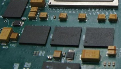
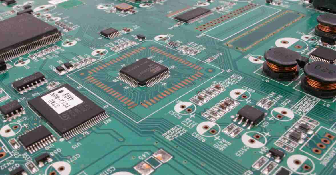
Blind hole circuit board, also known as HDI board, is often used in communication equipment, GPS navigation and other high-end products. This is a process that consists of internal and external circuits, re-drilling and metallization of the holes to realize the connection function between the internal circuits of each layer.
With the development of electronic products to high density and high precision, the same requirements are put forward for circuit boards. The most effective way to increase PCB density is to reduce the number of through-holes and precisely set blind and buried holes to achieve this requirement, resulting in the HDI board.
A blind hole is a hole that does not run through the circuit board. For example, in a 4-layer board, holes between the first and second layers, between the second and third layers, and so on. Circuit boards with blind holes are called blind holes.
With the development of portable product design towards miniaturization and high density, the blind buried hole of eight-layer circuit board puts forward higher requirements for PCB production process.
At present, most portable products, BGA package with spacing less than 0.65mm, and eight-layer blind hole control PCB board all adopt eight-layer circuit board blind hole buried blind hole process, so what is the blind hole process?
Blind hole: A blind hole is a hole that connects the PCB inner wiring to the PCB surface wiring. This hole does not penetrate the entire PCB circuit board.
Buried hole: A buried hole is a type of through hole that only connects the lines between the inner layers, so it is not visible from the PCB surface. The perforated plate is the same as the common double panel.
Blind hole plate, i.e. one side is the outer layer:
Positive process: need to do single-side d/f, must be careful not to reel wrong face (double-sided bottom copper is inconsistent); When d/f is exposed, the surface of the glossy copper is covered with black tape to prevent light transmission.
Because the blind hole plate has been made more than twice, the thickness of the finished product is easy to be too thick. Therefore, the graph should pay attention to the control of plate thickness and copper thickness, and the range of plate thickness and copper thickness should be marked after etching.
After pressing the plate, use the x-ray machine to punch out the target hole for the multilayer plate.
Negative film process: for sheet (<12mil copper) because it can not be produced in the electrogram pull, must be produced in water gold pull, and water gold pull can not be divided into the current, so can not according to the mi requirements to do single-side no current or small current. If the positive process is used, it often leads to excessive thickness of single-sided copper, resulting in etching difficulties and fine line phenomenon. Therefore, this kind of board needs to adopt the negative film process.
What is blind hole plate
Blind buried hole circuit board, also known as HDI board, is often used in communication equipment, GPS navigation and other high-end products. The structure of conventional multi-layer circuit board contains internal and external circuits, and the use of drilling, as well as the metallization process in the hole, to achieve the connection between the internal circuit layers.
With the development of electronic products to high density and high precision, the same requirements are put forward for circuit boards.


Just upload Gerber files, BOM files and design files, and the KINGFORD team will provide a complete quotation within 24h.