
Professional PCB manufacturing and assembly
Building 6, Zone 3, Yuekang Road,Bao'an District, Shenzhen, China
+86-13410863085Mon.-Sat.08:00-20:00

The printed circuit board(PCB) area dedicated to power management is a great constraint for system designers. Reducing conversion losses is a fundamental requirement to enable compact solutions in space-constrained applications with limited PCB base surfaces. The ability to flexibly deploy converters in strategic locations on the board is also important -- in the case of high-current load point (POL) modules, being in the best position adjacent to the load reduces on-off voltage drop and improves load transient performance.
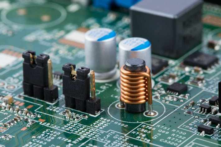
The improvement of component technology is the key to reduce the overall power consumption, especially the size reduction of filter passive components at higher switching frequencies. Power metal oxide semiconductor field-effect transistors (MosFets), for example, have seen consistent advances in silicon chips and packages, most notably with gallium nitride (GaN) power devices where parasitization is rare. At the same time, the performance of magnetic components has improved separately, although at a rate that may lag behind that of power semiconductor components. The careful layout of the control IC (integrated adaptive gate driver near the MOSFET) eliminates the need for power dissipation buffers or gate resistor assemblies to adjust the switching node voltage conversion rate in many cases.
While high-density layouts are generally good for improving conversion efficiency, they can create a cooling performance bottleneck. The idea of achieving the same power consumption in a smaller space becomes untenable. Higher failure rates and reliability problems are exacerbated by component temperature increases. Placing a slimmer looking power mosFets on top of the PCB (without being obscured by thicker components such as inductors and electrolytic capacitors) helps to improve heat dissipation through convective airflow. In the case of converters, inductors and electrolytic capacitors are deliberately placed at the bottom of the multilayer PCB, as they impede heat transfer if placed at the top.
EMI compliance is an important milestone in the product design cycle. High density designs usually have little room for EMI filtering. But a tight layout improves radiation emission and provides greater resistance to incoming interference. The two basic steps are to minimize the area of the loop carrying a large di/dt current and to reduce the surface area with a high dv/dt voltage.
The basic steps of the DC/DC converter PCB design process are:
1. Select PCB structure and cascading specifications.
2. Find the large di/dt current loop and the high dv/dt voltage node from the schematic diagram.
3. Lay out and place power level components.
4. Place the control IC and complete the layout of the control part.
5. Perform key tracking wiring, including MOSFET grid drive, current detection and output voltage feedback.
6. Design the power and grounding layers.
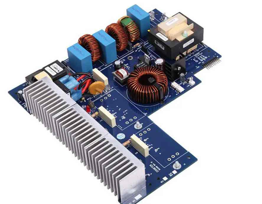
As an embedded POL module implementation, it employs an all-ceramic capacitor design, a high-efficiency shielded inductor, vertically stacked metal oxide semiconductor field effect transistors (MOSFETs), a voltage mode controller, and a 2-oz copper-clad six-layer PCB.
The main principle is to achieve high power density and low bill of Materials (BOM) cost. It occupies A total PCB area of 2.2cm2 (0.34in2) and produces an effective current density of 11.3A/cm2 (75A/in2) per unit area. The power density per unit volume at 3.3V output is 57W/in2 (930W/in3).
To achieve high power density, it is common practice to increase the switching frequency. In contrast, you can achieve miniaturization through strategic component selection while maintaining a low switching frequency of 300kHz, designed to reduce frequency-proportional losses such as MOSFET switching losses and inductor core losses. Achieve more functionality in a space-constrained design (reduced solution volume and space).
1. Reduce the parasitic inductance of the switching loop, reduce the voltage stress of the power MOSFET (voltage peak of the switching node) and chirp.
2. Reduce switch loss. Reduce electromagnetic interference (EMI), magnetic field coupling and output noise signals.
3. The extra tolerance ensures safe input rail transient voltage interference (especially in wide VIN range applications).
4. Increase reliability and robustness (reduce component temperature).
5. Save costs by shrinking PCB, reducing filter components, and removing buffers.
6. Distinctive design can provide competitive advantage, win customer attention and increase revenue.
The PCB layout determines the performance of a switched power converter. Of course, designers would be happy not to spend countless hours debugging EMI, noise, signal integrity, and other issues associated with poor layout.
Copper clad PCB circuit board solution
Feb 09,2023


Just upload Gerber files, BOM files and design files, and the KINGFORD team will provide a complete quotation within 24h.