
Professional PCB manufacturing and assembly
Building 6, Zone 3, Yuekang Road,Bao'an District, Shenzhen, China
+86-13410863085Mon.-Sat.08:00-20:00


In the process of PCB design, if possible risks can be predicted in advance and avoided in advance, the success rate of PCB design will be greatly improved. Many companies have a PCB design success rate when evaluating projects. Signal integrity design is the key to improve the success rate of a board. The following is with the embedded Xiaobian together to understand the relevant content.
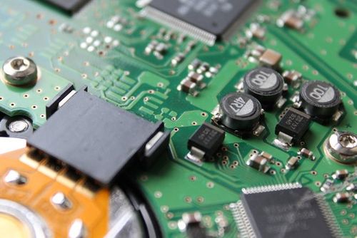
The current electronic system design, there are many product solutions, chip manufacturers have done, including what chip to use, how to build the peripheral circuit and so on. Most of the time, hardware engineers hardly need to consider the circuit principle, just need to make their own PCB.
But it is in the PCB design process, many enterprises have encountered difficulties, either the PCB design is not stable, or does not work. For large enterprises, many chip manufacturers will provide technical support and guidance for PCB design. However, some small and medium-sized enterprises find it difficult to get such support. Therefore, you have to find a way to complete, so there are many problems, may need to play several versions, debugging for a long time. In fact, if you know how the system is designed, it can be avoided. Let's talk about three tips to reduce the risk of PCB design.

First, in the system planning stage, it is best to consider the signal integrity problem. The whole system is built in this way, can the signal be correctly received from one PCB to another PCB? This should be evaluated in the early stage, and it is not very difficult to evaluate this problem, know a little signal integrity knowledge, can do a little simple software operation.
Second, in the process of PCB design, simulation software is used to evaluate the specific routing and observe whether the signal quality can meet the requirements. The simulation process itself is very simple. The key is to understand the principle knowledge of signal integrity and use it for guidance.
3. In the process of making PCB, risk control must be carried out. There are many problems, the simulation software has no way to solve, the designer must be artificial control. The key to this step is to know where the risks are and how to avoid them, which requires knowledge of signal integrity.
If you can grasp these three points in the process of PCB design, then PCB design risk will be greatly reduced, the probability of error will be much smaller after hitting the board, debugging is relatively easy.
PCB design: "Power supply plus magnetic beads" (second)
The relationship between the position of filter capacitor and the impedance of PDN is discussed, and the concepts of "global capacitance" and "local capacitance" are proposed. You can see that the position of the capacitor is not as important as you might think when it takes on "global characteristics".
This section: When the multilayer board is designed, the capacitor tends to present "global characteristics". The design method of "power supply plus magnetic beads" will affect the capacitor to play a role in the global scope. There are also other design problems with having too many types of power supplies.
From the previous article, we know that capacitors present "global characteristics" and "local characteristics" under different conditions of use.
To avoid the tedious research formula, let's look at the actual simulation results. In order to facilitate the study, a simulation case is designed, as shown in Figure 1: Case1 is the capacitor placed near the chip pin, and Case1b is the capacitor placed far away from the chip pin. At this time, Case1b has a pair of more power supply ground holes than Case1. In order to only compare the influence of the position of the capacitor under the same conditions, we add a pair of power supply ground holes to the same position as Case1b capacitor Fan out in case Case1a.
Let's first take a look at the situation when the ground distance of the power supply is 3mil: When the ground distance of the power supply is tightly coupled, the PDN curves of two cases A and b basically coincide, indicating that the resonant frequency of the capacitor does not change. In other words, the position of the capacitor seems to have almost no effect. On the contrary, the resonant frequency of Case1 tends to be low frequency, indicating that the installation inductance of Case1 is larger. This is easy to understand, mainly caused by an extra pair of power supply holes.
The above conclusions are similar when the power source ground distance is less than 10mil. However, when the power source is located at 20mil or even 50mil, the situation changes slightly. As shown in Figure 3, when the ground distance of the power supply increases, the PDN curves of Case a and Case b begin to deviate, and the resonant frequency of Case1b shifts to the low frequency, indicating that the installation inductance of the capacitor increases significantly when the capacitor is far away from the chip pin.


Just upload Gerber files, BOM files and design files, and the KINGFORD team will provide a complete quotation within 24h.