
Professional PCB manufacturing and assembly
Building 6, Zone 3, Yuekang Road,Bao'an District, Shenzhen, China
+86-13410863085Mon.-Sat.08:00-20:00

After years of development, the PCB industry has also extensively upgraded its processes and capabilities. Due to technical requirements, some PCB processing processes that were previously considered exotic will soon be considered routine. Of course, it depends on many other issues as well. Due to the nature of emerging and evolving applications, the PCB industry may need to make more advances in some processes.
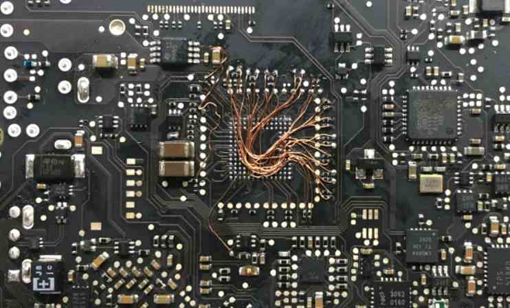
PCB processors that process 77 GHz automotive radar PCB or antennas are well aware of the stringent requirements for ultra-high frequency applications. Generally, applications at higher frequencies become sensitive to some PCB processes and their normal tolerance variations. A simple example is the etching accuracy of the circuit, conductor width usually needs to have more strict tolerances, the trapeze shape of the signal conductor is usually specified to a certain range, even the roughness of the conductor side will cause the difference in radio frequency performance at 77GHz, copper plating thickness changes may also cause a big problem. Therefore, strict control of the process is very important for UHF applications.
There are new applications over 77 GHz that require processing capabilities beyond existing PCB technologies. For example, for the 140 GHz currently being used around specific applications, the conductor width tolerance needs to be controlled to ±1um (0.04 mil), the conductor thickness needs to be very thin (2 um), and the thickness variation needs to be controlled to ±0.5um. There are other metrics (e.g., ultra-strict position tolerances between circuit patterns and microholes, interlayer alignment, etc.) that are difficult or may not be achievable with existing printed circuit board.
Several 140 GHz applications are known, one of which uses PCB technology and semiconductor technology. The motherboard is made with PCB technology, the highest working frequency of the circuit board is 35GHz, the circuit board for the current PCB processing without any problems, completely can meet the requirements. The motherboard is then fitted with a small glass circuit made using semiconductor technology, which has a row of slots at the edges for welding to the motherboard. The 35GHz signal from the PCB board is transferred to the glass circuit through the slot channel, which is shifted to about 140 GHz by a 4x frequency multiplier. The 140 GHz signal is then processed on a glass-based circuit as needed. While the 140GHz is a very interesting design, I am more skeptical about its mass production capability and cost.
Laser conductor processing technology can also be used as a PCB processing technology. Some of the latest laser conductor fabrication techniques can generate high precision circuit geometers. Currently, there are some limitations to these processes, but over time, and if the PCB industry applies the laser conductor process to mass production, it may become a future process for millimeter-wave PCB circuits.
Another PCB process that may benefit the further development of the PCB industry is welding technology. Welding technology has been around for years, but has not usually been used in mass production. There are a number of aspects to overcome to make the technology suitable for mass production, while maintaining the electrical properties it can provide. The welding technique requires the use of tightly controlled laminating equipment and processes to essentially melt the thermoplastic material to be used as a bonding material for multilayer circuits. For engineers who have been working with different high frequency materials, one material with the best electrical properties, especially for high frequency applications, is PTFE-based. However, to use PTFE - based bonding materials to manufacture multilayer plates, it is necessary to use the welding process


Just upload Gerber files, BOM files and design files, and the KINGFORD team will provide a complete quotation within 24h.