
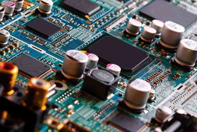
Professional PCB manufacturing and assembly
Building 6, Zone 3, Yuekang Road,Bao'an District, Shenzhen, China
+86-13410863085Mon.-Sat.08:00-20:00

SignalLayers:
Signal layers include TopLayer, Bottom Layer, Mid Layer 1... 30. These layers are all layers with electrical connections, which is the actual copper layer. Intermediate layer refers to the intermediate plate layer used for wiring, in which the wire is distributed.
Internal Plane:
Internal Plane 1... 16, this type of layer is only used for multilayer board, these layers are generally connected to the ground and power supply, become the power layer and the stratum, also has the electrical connection function, is also the actual copper layer, but the layer is generally not wired, is composed of the whole copper film.
SilkscreenOverlay: SilkScreenOverlay:
It includes Top overlay layer and Bottom overlay layer. The definition of the top and bottom screen characters is generally printed on the solder resistance layer of some text symbols, such as component name, component symbol, component pin and copyright, for the convenience of later circuit welding and error checking.
PasteMask:
The auxiliary paste layer, including the Top paste layer and the Bottom paste layer, refers to the exposed surface of the solder plate that we can see, that is, the part of the solder paste that needs to be applied before welding. Therefore, this layer is also useful in hot air leveling of the pad and making welding steel mesh.
SolderMask:
Including Top solder and Bottom solder, which is opposite to solder, referring to the layer to be covered with green oil. The layer does not stick to solder to prevent excess solder at adjacent welding points from short-circuiting during welding. The solder resistance layer covers the copper film wire to prevent the copper film from oxidizing too quickly in the air, but leaves a position at the solder joint and does not cover the solder joint. The solder shield is used to match the pad during the design process and is automatically generated.
MechanicalLayers:
Up to 16 machining layers can be selected. To design a double panel, just use the default Mechanical Layer 1.
The mechanical layer defines the appearance of the entire PCB board. It is used to set the board dimensions, data marks, alignment marks, assembly instructions, and other mechanical information. Design for PCB mechanical shape, default LAYER1 is the shape layer. Other LAYER2/3/4 etc. can be used for mechanical dimensioning or special purposes. For example, when some boards need to make conductive carbon oil, LAYER2/3/4 etc. can be used, but the purpose of the layer must be clearly marked on the same floor.
Keep Out Layer: Keep out layer:
Define the boundaries of the wiring layer. After the forbidden wiring layer is defined, the wiring with electrical characteristics shall not exceed the boundary of the forbidden wiring layer in the future wiring process. Many designers also use PCB MECHANICAL shape. If there are KEEPOUT and MECHANICAL LAYER1 on the printed circuit board at the same time, the integrity of the two layers is mainly looked at. Generally, MECHANICAL LAYER1 shall prevail. It is suggested that MECHANICAL LAYER1 should be used as the outline LAYER as far as possible in the design. If KEEPOUT LAYER is used as the outline, do not use MECHANICAL LAYER1 again to avoid confusion! Drill Layer: Including Drill guide and Drill data drawing, drill data. The borehole layer provides information about the boreholes in the circuit board manufacturing process (e.g., solder pads, which require boreholes). Protel 99 SE provides two Drill layers, Drill gride(drill indication drawing) and Drill drawing(drill drawing).
Multi-layer:
Refers to all layers of PCB circuit board. The solder plate on the circuit board and through the hole to penetrate the whole circuit board, and different conductive graphic layer to establish electrical connection relationship, so the system is specially set up an abstract layer - layer. Generally, the pad and the hole should be set on the multilayer, if the layer is closed, the pad and the hole can not be displayed.
The distinction between solder resistance and solder aid
Welding resistance layer: soldermask, refers to the part of the board to be green oil; Because it is a negative output, the part of solder mask is not solder oil, but silver-white.
Welding layer: pastemask, is used when the machine patch, is corresponding to all the patch components of the pad, the size of the toplayer/bottomlayer, is used to open the steel mesh with tin leakage.
Key points: Both layers are used for soldering on tin, not referring to a tin, a green oil; So is there a layer refers to the layer of green oil, as long as there is a layer on an area, it means that the area is insulated green oil? I haven't come across such a layer yet! The solder plate on the PCB board we painted will all solder layer by default. Therefore, the solder plate on the PCB board manufactured is coated with silver solder, and it is not surprising that there is no green oil. However, the wiring part on the PCB board we drew only has toplayer or bottomlayer layer, rather than solder layer, but the wiring part of the PCB board made is coated with green oil.
It can be understood in this way: 1. The solder resistance layer means that the window is opened on the green oil of the whole piece of solder resistance, in order to allow welding! 2. By default, green oil should be applied to areas without solder resistance layer! 3. paste mask layer is used for patch encapsulation! SMT packaging uses toplayer layer, topsolder layer, and toppaste layer. toplayer and toppaste are the same size, but toppaste is larger than them. The DIP package is used only for: topsolder and multilayer layer (after decomposition, I found that multilayer is actually toplayer, bottomlayer, topsolder, bottomsolder layer overlapping), topsolder/bottomsolder is larger than toplayer/bottomlayer.
The welding pad will open a window by default in the design (OVERRIDE: 0.1016mm), that is, the welding pad is exposed to copper foil, and the outer expansion is 0.1016mm, and the tin will be raised during wave soldering. No design changes are recommended to ensure weldability;
The overhole will be windowed by default in the design (OVERRIDE: 0.1016mm), that is, the overhole copper foil will be expanded by 0.1016mm and will be tinned during wave soldering. If the design is to prevent SOLDER from passing through the hole, do not expose copper, you must check the PENTING option of SOLDER MASK (solder window) to close the pass through the hole window.


Just upload Gerber files, BOM files and design files, and the KINGFORD team will provide a complete quotation within 24h.