
Professional PCB manufacturing and assembly
Building 6, Zone 3, Yuekang Road,Bao'an District, Shenzhen, China
+86-13410863085Mon.-Sat.08:00-20:00

I. Overview
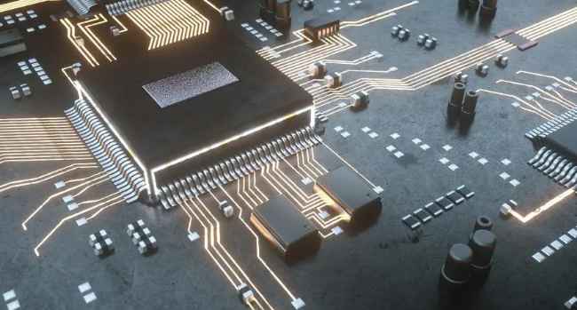
At present, the typical process of printing circuit board (PCB) processing is "graphic plating method". That is, on the copper foil part of the outer layer of the board to be retained, that is, on the graphic part of the circuit, a layer of lead tin corrosion resistance layer is pre-plated, and then the rest of the copper foil is etched away by chemical means, which is called etching. Note that there are two layers of copper on the board. In the outer etching process only one layer of copper must be etched away; the rest will form the final circuit needed. This type of graphic plating is characterized by the presence of a copper coating only under the lead tin resist layer. Alternatively, the entire plate is coated with copper, with only tin or lead-tin resist outside the film (see Figure 3). This process is called "full plate copper plating process". The biggest disadvantage of full plate copper plating, compared with graphic plating, is that it has to be plated twice on each side of the plate and must be corroded away during etching. So there's a whole series of problems when the wire width is very fine. Meanwhile, side corrosion (see Figure 4) will seriously affect the uniformity of the lines.
In the processing of the outer circuit of the printed board, there is another method, is to use the sensitive film instead of the metal coating as the corrosion resistance layer. This method is very similar to the inner etching process, see Etching in Inner fabrication process. At present, tin or lead tin is the most commonly used corrosion resistance layer, used in the etching process of ammonia etching agents. Ammonia etching agent is a commonly used chemical liquid which does not have any chemical reaction with tin or lead tin. Ammonia etching agent mainly refers to ammonia water/ammonia chloride etching solution. In addition, ammonia/ammonia sulfate etching solution is available on the market.
Sulfate-based etching solution in which the copper can be separated by electrolysis after use and thus can be reused. Due to its low corrosion rate, it is rarely seen in actual production, but it is expected to be used in chlorine free etching. Some people experiment with sulfuric acid - hydrogen peroxide as etching agent to etch the outer pattern. This process has not yet been adopted in a commercial sense for a number of reasons, including economic and liquid waste disposal. Furthermore, sulfuric acid-hydrogen peroxide, can not be used for etching lead tin corrosion resistance layer, and this process is not the main method in the production of PCB outer layer, so most people rarely care about it.

Ii. Etching quality and previous problems
The basic requirement for etching quality is to be able to completely remove all layers of copper except under the resist layer, and that is all. Strictly speaking, if it is to be defined precisely, then the etching quality must include the consistency of the wire width and the degree of lateral erosion. Due to the inherent characteristics of the present corrosion fluid, not only downward but also to the left and right direction of the etching action, so the side erosion is almost inevitable.
The problem of lateral erosion is one of the etch parameters which is often discussed. It is defined as the ratio of lateral erosion width to etching depth, which is called etching factor. In the printed circuit industry, it varies widely, from 1:1 to 1:5. Obviously, small side etch or low etching factor is the most satisfactory.
The structure of the etching equipment and the different composition of the etching solution can affect or control the etching factor or the degree of lateral erosion. The side erosion can be reduced by some additives. The chemical composition of these additives is generally a trade secret, and the respective developers are not disclosed to the outside world. As for the structure of the etching equipment, a later section will be devoted to that.
In many ways, the quality of etching has existed long before the printed board entered the etching machine. Because there is a very close internal relationship between each process or process of printed circuit processing, there is no one is not affected by other processes and does not affect other processes. Many of the problems identified as etching quality actually exist in the process of membrane removal and even before. For the etching process of the outer layer graphics, because it reflects the "reverse stream" image than most printed board processes are prominent, so many problems are reflected in it. At the same time, this is also because etching is the last link in a long series of processes that start with self-laminating, sensitization, after which the outer pattern is transferred successfully. The more links there are, the more likely there will be problems. This can be regarded as a very special aspect of the printed circuit production process.
Theoretically speaking, the printed circuit into the etching stage, its graphic cross-section state should. In the process of graphic electroplating processing printed circuits, the ideal state should be: the sum of the thickness of copper and tin or copper and lead tin after electroplating should not exceed the thickness of the electroplating sensitive film, so that the electroplating graphics are completely blocked by the "wall" on both sides of the film and embedded in it. However, in reality, the printed circuit board in the world after electroplating, coating pattern is much thicker than the sensitive pattern. The problem arises in the plating of copper and lead tin, when the coating is higher than the photosensitive film and tends to accumulate laterally. A tin or lead tin resist covering the top of the line extends to both sides, forming a "rim" that covers a small portion of the sensitive film underneath the "rim"
Why did these PCB companies fail?
Feb 05,2023


Just upload Gerber files, BOM files and design files, and the KINGFORD team will provide a complete quotation within 24h.