
Professional PCB manufacturing and assembly
Building 6, Zone 3, Yuekang Road,Bao'an District, Shenzhen, China
+86-13410863085Mon.-Sat.08:00-20:00


Depending on the design of the circuit board, the price will be determined by the material of the circuit board, the number of layers of the circuit board, the size of the circuit board, the number of each production, the production process, the minimum line width and line distance, the minimum aperture and the number of holes, the special process and other requirements.
There are mainly the following ways to calculate prices in the industry:
1. Calculate the price by size (applicable to small batch of samples)
The manufacturer will give the unit price per square centimeter according to different circuit board layers and different processes. The customer only needs to change the size of the circuit board into centimeters and then multiply the unit price per square centimeter to get the unit price of the circuit board to be produced. This calculation method is very suitable for the ordinary process of the circuit board, both convenient manufacturers and buyers. Here are some examples:
For example, a manufacturer pricing single panel, FR-4 material, 10-20 square meters of the order, the unit price is 0.04 yuan/square centimeter, then if the buyer's circuit board size is 10*10CM, the production quantity is 1000-2000 pieces, just meet this standard, the unit price is equal to 10*10*0.04=4 yuan a piece.
2. Calculate the price by cost refinement (for large quantities)
Because the raw material of the circuit board is copper clad plate, the production of copper clad plate factory set some fixed size on the market sales, common 915MM*1220MM (36"*48"); 940MM*1245MM (37"*49"); 1020MM*1220MM (40"*48"); 1067mm*1220mm (42"*48"); 1042MM*1245MM (41"49"); 1093MM*1245MM (43"*49"); The manufacturer will calculate the copper clad utilization rate of this batch of circuit boards according to the materials, layers, processes, quantity and other parameters of the circuit boards to be produced, so as to calculate the material cost. For example, if you produce a circuit board of 100*100MM, the factory may assemble large boards of 100*4 and 100*5 to improve production efficiency. Among them, they also need to add some spacing and plate edge for convenient production. Generally, the spacing of gong plate is 2MM, and the plate edge is 8-20MM, and then the large plate formed is cut in the size of the raw material. Here, if it is just cut and there is no excess plate, it is to maximize the utilization rate. Figuring out the utilization is just one step. You also have to figure out the drilling cost, see how many holes there are, how big the smallest hole is, how many holes there are in a big plate, figure out the cost of each small process such as copper plating based on the lines in the board, and finally add the average labor cost, attrition rate, profit margin, marketing expenses for each company. Finally, divide the total cost by how many small plates can be produced from a large piece of raw material to find the unit price of small plates. This process is very complex, the need to have a special person to do, the general offer will take more than a few hours.
3. Online meter
Because the price of circuit board is affected by a variety of factors, ordinary purchasers do not understand the quotation process of suppliers, often to get a price takes a long time, waste a lot of manpower and material resources, but also because they want to know the price of a circuit board, the personal contact information to the factory to bring follow-up marketing harassment. Many companies have started to set up a circuit board pricing program on their Web sites, with rules that allow customers to freely calculate prices. People who do not understand PCB can also easily calculate the price of PCB.

Composition:
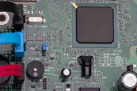
The circuit board is mainly composed of welding pad, through hole, mounting hole, wire, components, connectors, filling, electrical boundary, etc. The main functions of each component are as follows:
Pad: Metal hole for welding the pin of a component.
Through holes: there are metal through holes and non-metal through holes, wherein metal through holes are used to connect the pins of components between each layer.
Mounting hole: used to secure the circuit board.
Wire: Electrical network copper film used to connect the pins of a component.
Connector: A component used to connect circuit boards.
Filling: Copper applied to ground wire network can effectively reduce impedance.
Electrical boundary: Used to determine the size of the circuit board. All components on the circuit board must not exceed this boundary.
Main categories:
Circuit board systems are classified into the following three types:
Single panel
Single-Sided Boards
We just mentioned that, so we're going to call this type of PCB Single-sided. Only early circuits used such boards because single panels had many severe limitations on the design circuit (because they had only one side, the wires could not cross and had to go around a separate path).
Double panel
Double-Sided Boards
The circuit board has wiring on both sides. But to use both wires, there must be a proper circuit connection between the two sides. This "bridge" between circuits is called a pilot hole (via). A pilot hole is a small hole in a PCB filled with or coated with metal that can be connected to wires on both sides. Because the area of a dual panel is twice as large as that of a single panel, and because the wiring can be interleaved (it can go around to the other side), it is better suited for more complex circuits than a single panel.
Multilayer board
[Multilayer board] For more complex applications, the circuit can be arranged into a multi-layer structure and pressed together, and in the layers laid through the circuit to connect each layer circuit.
Inner circuit
Copper foil substrate is first cut to size suitable for processing production. Before pressing the substrate film, it is usually necessary to coarse the copper foil on the surface of the substrate properly by brush grinding, micro-etching and other methods, and then attach the dry film photoresist tightly to it at the appropriate temperature and pressure. The substrate pasted with dry film photoresist is sent to the UV exposure machine for exposure. The photoresist will produce polymerization reaction after ultraviolet irradiation in the film transmittance area (the dry film in this area will be retained as etching resistance in the later development and copper etching steps), and the line image on the negative will be transferred to the dry film photoresist on the surface of the plate. After tearing off the protective adhesive film on the film surface, the development of the unilluminated area on the film surface is removed with sodium carbonate aqueous solution, and then the exposed copper foil is corroded and removed with hydrochloric acid and hydrogen peroxide mixed solution to form a circuit. Finally, the successful dry film was photoresist washed with sodium hydroxide aqueous solution. For more than six layers (including) of the inner circuit board with automatic positioning punching machine out of the interlayer line alignment of the riveting reference hole. Multi-Layer Boards
In order to increase the area that can be wired, more single or double sided wiring boards are used in multilayer boards. Multilayer plates are made of several double panels, and a layer of insulation is placed between each layer of plates and glued firmly (pressed together).
The number of layers on the board means that there are several separate wiring layers, usually with an even number of layers, including the two outermost layers. Most main boards are built with 4 to 8 layers, but technically close to 100 layers of PCB boards are possible. Most large supercomputers use quite a few layers of mainframe boards, but because such machines can be replaced by clusters of ordinary computers, super-multiboards have fallen out of use. Because the layers in a PCB are so tightly integrated, it is not always easy to see the actual number, but if you look closely at the host board, you may be able to see it.


Just upload Gerber files, BOM files and design files, and the KINGFORD team will provide a complete quotation within 24h.