
Professional PCB manufacturing and assembly
Building 6, Zone 3, Yuekang Road,Bao'an District, Shenzhen, China
+86-13410863085Mon.-Sat.08:00-20:00


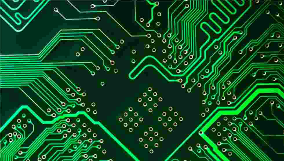
With the decrease of signal rising time and the increase of signal frequency, the EMI problem of electronic products will be more and more noticed by electronic engineers. With the success of high-speed PCB design, the contribution to EMI has been paid more and more attention. Almost 60% EMI problems can be controlled and solved by high-speed PCB.
Rule 1, Rules for masking high-speed signal cabling:
In high-speed PCB design, key high-speed signal lines, such as clocks, need to be screened for routing. If not screened or only partially screened, EMI leakage will be caused. It is recommended that shielded cables be drilled and grounded every 1000mil.
Rule 2, closed-loop rule of high-speed signal routing:
Due to the increasing density of PCB board, many PCB LAYOUT engineers are easy to make such mistakes in the process of wiring.
Due to the increasing density of PCB board, it is easy for many PCB LAYOUT engineers to make a mistake in the process of wiring, that is, high-speed signal network such as clock signal generates a closed-loop result when multi-layer PCB is wiring. Such closed-loop result will generate a ring antenna and increase the radiation intensity of EMI.
Rule 3: open-loop rule for high-speed signal routing:
Rule two mentions that a closed loop of a high-speed signal will cause EMI radiation, while an open loop will also cause EMI radiation.
High-speed signal networks, such as clock signals, will generate linear antennas and increase EMI radiation intensity once the open-loop result is generated during the wiring of multi-layer PCB.
Rule 4, characteristic impedance continuity rule of high-speed signal:
High-speed signals must ensure the continuity of characteristic impedance when switching between layers, otherwise EMI radiation will be increased. In other words, the width of the wiring in the same layer must be continuous, and the impedance of the different layers must be continuous.
Rule 5, wiring direction rules for high-speed PCB design:
The cables between two adjacent layers must be routed vertically. Otherwise, cross-talk will occur between the two layers and EMI radiation will be increased.
In short, adjacent wiring layers follow the direction of horizontal, horizontal and vertical, and vertical wiring can suppress crosstalk between lines.
Rule 6, topological structure rules in high-speed PCB design:
In high speed printed circuit board design, the circuit board characteristic impedance control and multi-load topology design directly determine the success or failure of the product.

Rule 7: Resonance rule of wire length:
Check whether the length of the signal line and the frequency of the signal constitute resonance, that is, when the length of the wiring is an integer multiple of the signal wavelength of 1/4, the wiring will generate resonance, and the resonance will radiate electromagnetic waves, resulting in interference.
Rule 8: Reflux path rules:
All high speed signals must have a good return path. As far as possible, the return path of high-speed signal such as clock is minimized. Otherwise, it will greatly increase the radiation, and the radiation size is proportional to the area surrounded by the signal path and the return path.
Rule 9, the decoupling capacitor placement rules of the PCB circuit board device:
The location of the decoupling capacitor is very important. Improper placement does not have the effect of decoupling. The principle is: close to the pin of the power supply, and the capacitance of the power supply and ground surrounded by the minimum area.


Just upload Gerber files, BOM files and design files, and the KINGFORD team will provide a complete quotation within 24h.