
Professional PCB manufacturing and assembly
Building 6, Zone 3, Yuekang Road,Bao'an District, Shenzhen, China
+86-13410863085Mon.-Sat.08:00-20:00

Thoughts on Failure Analysis of PCB and PCBA
PCB manufacturers know that in the failure analysis of practical reliability problems, PCB failure mechanisms are complex and diverse, so SMT technology engineers need to have correct analysis ideas in case investigation Careful logical thinking and various analysis tools are required to find the real cause of the fault PCB In this process, if there is any negligence in any link, it is likely to cause "unfair" situations, false and wrong cases "
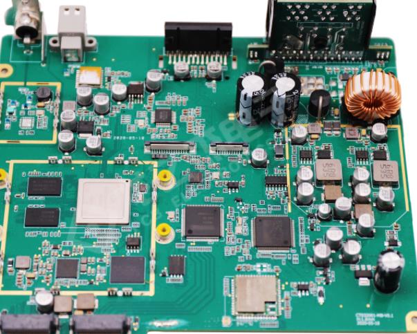
Pcb and PCBA

General analysis ideas of reliability problems
1. PCB background information collection
The background information of PCB is the basis of reliability failure analysis, which directly affects the trend of all subsequent failure analysis and has a decisive impact on the final decision-making of the mechanism.
Recall that before fault analysis, the information behind PCB faults should be collected as much as possible, usually including but not limited to:
1) PCB fault range: fault batch information and corresponding fault rate
(1) If problems occur in a single batch or the failure rate is low during the production of a large number of PCB boards, the possibility of abnormal process control is high;
(2) If the first or more batches have problems or high failure rate, the influence of data and design factors shall not be excluded;
2) Pre failure treatment of PCB: whether PCB or PCBA has undergone a series of pretreatment before failure; Common pre-treatment includes baking before reflow. Is there lead reflow? Lead wave soldering and manual soldering can be used. If necessary, detailed information about the solder paste used in each pretreatment process is required. Wire mesh. Tin wire, etc.). Equipment iron power, etc.) and parameter return curve. Peak welding parameters. Manual welding temperature) information;
3) Fault scenario: specific information about PCB or PCBA faults, some of which are invalid during preprocessing, such as welding assembly, such as poor solderability. Layering, etc. Others are aging. The test even fails during use, such as CAF. ECM。 Circuit board, etc; SMT engineers need to know more about the failure process and relevant parameter data.
Failure Analysis of PCB/pcba
Generally speaking, the number of PCB failures is limited, even only one. In this regard, the analysis of PCB failure must follow the principle of layer by layer analysis from outside to inside, from nondestructive to destructive. Special attention must be paid to the analysis of PCB process, and the failure location should not be damaged prematurely:
1) Appearance observation
Appearance observation is the first step to analyze PCB faults. By combining the appearance and background information of the fault site, experienced fault analysis engineers can basically determine the number of possible fault causes and conduct targeted follow-up analysis. However, it is worth noting that there are many ways to observe the appearance, including visualization. Hand held magnifying glass. Desk magnifier. Stereomicroscope and metallographic microscope, etc. However, due to the light source. For different imaging principles and observation depths, it is necessary to analyze the morphology observed by corresponding equipment in combination with equipment factors. Never make a subjective guess with a preconceived idea, which will lead to the wrong direction of PCB failure analysis and waste valuable invalid products and analysis time.
2) Depth non-destructive analysis
Some PCB faults can not collect enough PCB fault information or even find fault points, such as delamination, only through visual observation. Virtual welding and internal openings require additional non-destructive analysis to further gather information, including ultrasonic testing. 3D X-ray. Infrared thermal imaging. Short circuit position detection, etc.
During appearance observation and non-destructive analysis, attention shall be paid to the common or different characteristics of different faulty products, which can be used as a reference for subsequent fault judgment. After sufficient information is collected in the damage analysis phase, target damage analysis can be started.
3) Damage analysis
Failure analysis of PCB is an essential and particularly critical step, which often determines the success of failure analysis. There are many methods for damage analysis, such as scanning electron microscopy and element analysis. Horizontal/vertical slice. FTIR, etc. At this stage, although the fault analysis method is very important, it is more important for SMT technicians to insight and judge the defects of PCB, correctly and clearly understand the fault mode and mechanism, and find the real cause of PCB fault.
Bare PCB analysis method
When the failure rate of PCB board is very high, the analysis of bare PCB board is also very necessary, which can be used as a supplement to the failure cause analysis. When the fault of PCB in the analysis phase is caused by the defect of bare PCB, which leads to further reliability fault, the bare PCB has the same defect. After the same processing process as the fault product, it will reflect the same fault mode as the fault product. If the same failure mode does not occur, the cause analysis of product loss is incorrect, at least incomplete.
Copy Test
When the failure rate is very low and no help can be obtained from the bare PCB analysis, it is necessary to reproduce the defects of the PCB and further reproduce the failure mode of the failed product, so that the failure analysis can form a closed loop.
In the face of increasing reliability failure PCB design optimization failure analysis Process improvement Data selection provides important first-hand information and is the starting point for reliability growth
SMT process specification for PCBA manufacturing
Dec 01,2022


Just upload Gerber files, BOM files and design files, and the KINGFORD team will provide a complete quotation within 24h.