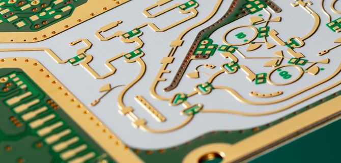
Calculation Method for Manufacturing Cost of Multilayer Printed Circuit Board
When ordering multilayer printed circuit boards, you must ensure that they are purchased at a reasonable cost However, most customers who need them only consider the total price, including cost
Helping customers reduce the cost of multilayer PCB in the manufacturing process is the primary task of many manufacturers. However, multilayer PCB customers can learn how to reduce costs in the manufacturing process of multilayer PCB through simple methods or means. Here are 9 effective ways to help multi-layer correct PCB service providers reduce costs. Fortunately, there are various PCB manufacturing.
Multilayer board specification
The trace width is important because the correct trace width can ensure that the trace (whether power or signal) will operate as required and provide the best function of the printed circuit board. However, in general, the width of the track carrying the logo may be less than the width of the track used to carry the current.
Customers who order multilayer printed circuit boards can reduce related costs or buy cheaply by ensuring that manufacturers reduce track width and spacing. Unfortunately, most customers do not realize that problems related to track width and spacing at the design stage will significantly affect their PCB costs. To ensure that manufacturing costs remain low, you need to select a size that provides you with comfortable space to complete the layout.
It should be noted that the closer the spacing is, the higher the manufacturing cost of PCB design is. Although trace and width spacing are basic features, especially on multilayer printed circuit boards, it is necessary to reduce trace and width spacing.
Circuit board

Track width and spacing
The trace width is important because the correct trace width can ensure that the trace (whether power or signal) will operate as required and provide the best function of the printed circuit board. However, in general, the width of the track carrying the logo may be less than the width of the track used to carry the current.
Customers who order multilayer printed circuit boards can reduce related costs or buy cheaply by ensuring that manufacturers reduce track width and spacing. Unfortunately, most customers do not realize that problems related to track width and spacing at the design stage will significantly affect their PCB costs. To ensure that manufacturing costs remain low, you need to select a size that provides you with comfortable space to complete the layout.
It should be noted that the closer the spacing is, the higher the manufacturing cost of PCB design is. Although trace and width spacing are basic features, especially on multilayer printed circuit boards, it is necessary to reduce trace and width spacing.
Plating and finishing
When multi-layer printed circuit boards are involved, another factor to consider is the cost associated with electroplating and surface treatment. Some surface treatments make high-end multilayer printed circuit boards have a longer shelf life, thus increasing manufacturing costs. HASL is one of the most advantageous and extremely low-cost finishes.
If you want to reduce the production cost of multilayer PCB, make sure to use cheaper electroplating and finishing programs Not all of these are low cost For example, surface treatment procedures such as electroless nickel plating and gold leaching are expensive, especially in the case of limited budget
Mass production
Before mass production became popular, the creation of PCB products with the most layers highly depended on the initial order However, when mass production is developed and improved, most companies see the advantages or benefits of mass production In other words, mass production reduces manufacturing costs Mass production of products is cheaper than the production of single parts with economies of scale
This is also true when manufacturing multilayer printed circuit boards. If you want to reduce manufacturing costs, you need to mass produce printed circuit boards. Through this pipeline, you will reduce or minimize the total cost of producing each product.
Limit the number of geometry
If you want to reduce the cost of manufacturing multilayer printed circuit boards, you must ensure that the geometry is reduced. The geometry does describe the dielectric substrate details, reference planes, and traces in the PCB stack.
If you choose to use or have larger geometry, this will lead to higher prices, especially in terms of the overall number of printed circuit boards. Although larger geometries will lead to higher yields, you must be prepared to spend more on multilayer printed circuit boards.
Observe recommended tolerances
Although the tolerance is strict, especially the thickness of printed circuit boards, it can achieve high-performance printed circuit boards. You need to note that this will increase the cost of new layers of films on printed circuit boards in the manufacturing stage
Remember, as a customer who wants to reduce the manufacturing cost of multilayer printed circuit boards, it is best to select only strict tolerances that are conducive to PCB design and efficiency. Otherwise, it is better to limit the thickness of the circuit board to the tolerance range. You need to follow the recommended tolerances to ensure that manufacturing costs are reduced.
Maintain sufficient spacing between copper layers
More than half an ounce of copper in the inner layer of PCB and nearly one ounce of copper in the outer layer of PCB significantly increase the manufacturing cost of PCB.
In order to ensure that the manufacturing cost of multilayer printed circuit boards is greatly reduced, you need to ensure that there is enough space between copper materials. To ensure that the cost of multilayer printed circuit boards is reduced, you may need to instruct manufacturers to use thick copper. If the spacing between copper materials is far different, it means that you will have to use a large number of components, which will increase the cost of manufacturing printed circuit boards.
Drilling size for multi-layer PCB manufacturing
In the manufacture of printed circuit boards, the type of machine or equipment used to drill holes in printed circuit boards is very important. Although high speed and flexibility are some of the most important advantages of laser drilling machines, you need to be aware that using these types of equipment will increase your manufacturing costs.
If you want to significantly reduce the manufacturing costs associated with manufacturing multilayer printed circuit boards, consider using nominal size drill holes instead of laser drill holes, unless laser is the only viable option. When designing multilayer printed circuit boards, larger apertures are required because they require lower accuracy, especially in multilayer PCB manufacturing. In addition, this will reduce your manufacturing costs for multilayer PCBs.
Multi layer PCB manufacturing PCB data selection
Finally, the choice of materials used to manufacture printed circuit boards, especially multilayer printed circuit boards, always affects production costs. Some factors affecting data selection include temperature reliability, thermal reliability, signal efficiency, heat transfer and mechanical efficiency.
Based on experience, those operations involving high frequency will require advanced information If you have a limited budget and want to minimize the manufacturing cost of multilayer PCB, then, it is recommended that you select cost-effective materials suitable for your application If you use high-end equipment and require the final product to have a good surface finish, you must be prepared for the high production costs associated with such programs


