
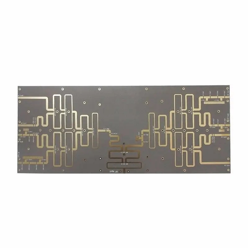
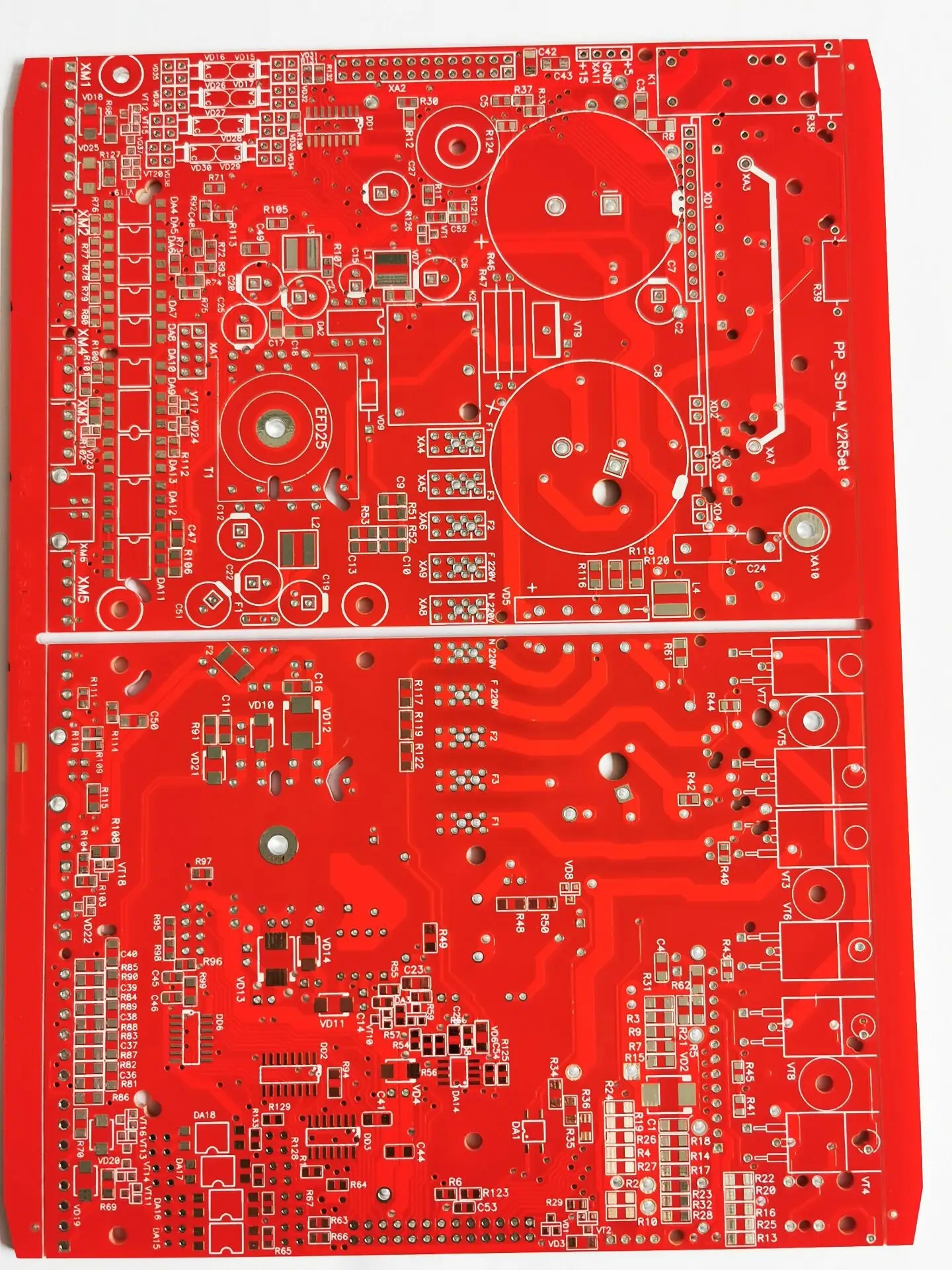
Professional PCB manufacturing and assembly
Building 6, Zone 3, Yuekang Road,Bao'an District, Shenzhen, China
+86-13410863085Mon.-Sat.08:00-20:00

Attention Problems in PCB Proofing Process and PCB Process Flow
First, pay attention to the number of samples
Before large-scale mass production, enterprises often need to make a batch of PCB templates for testing, which actually accounts for a certain cost of the enterprise. Especially when the enterprise is large in size and produces many types of PCB, the cost of PCB proofing and testing is also very considerable. From this point of view, enterprises should pay attention to the number of samples during PCB proofing.
Second, confirm the device packaging
Welding chips with specific functions on the circuit board and packaging them with shielding cover is a process in the circuit board manufacturing process. In the process of PCB proofing, the entrusting party should pay great attention to whether the internal chips and electronic components are wrongly soldered during packaging, so as to ensure the quality of PCB proofing, and then the normal verification function and subsequent further large-scale production can be achieved.
III. Comprehensive electrical inspection
After PCB proofing, the enterprise should conduct a comprehensive electrical inspection to ensure that every function and every detail of the PCB are checked, which is the significance of PCB proofing and the guarantee of whether the subsequent PCB can be put into mass production and ensure extremely low defective rate. To conduct a comprehensive electrical inspection, it is recommended that the entrusting party cooperate with the sampling party to carry out a more rigorous test method.
Of course, there are still some signal integrity layouts that need to be paid attention to and solved by both parties, but generally speaking, the problems that need to be paid attention to in PCB proofing are roughly the above items. Although there are many doubts about what PCB proofing means in the market, as an insider, doing a comprehensive troubleshooting and testing of the above issues is the basis for ensuring the quality of PCB samples and transforming them into subsequent mass production. PCB proofing must be treated seriously.
PCB process flow, understand after reading!
1. Cut
Cutting is the process of cutting the original CCL into boards that can be made on the production line.
First, let's understand several concepts:
(1) UNIT: UNIT refers to the cell graphics designed by PCB design engineers.
(2) SET: SET refers to a graphic that engineers put together multiple UNITs to improve production efficiency and facilitate production. It is also called panel, which includes unit graphics, process edges, etc.
(3) PANEL: PANEL refers to a board made up of multiple SET and tool board edges to improve efficiency and facilitate production.
2. INNER DRY FILM
The inner layer dry film is the process of transferring the inner layer circuit pattern to the PCB board.
In PCB production, we will mention the concept of pattern transfer, because the production of conductive patterns is fundamental to PCB production. Therefore, the graphic transfer process is of great significance for PCB fabrication.
The inner dry film includes multiple processes such as inner film pasting, exposure and development, and inner etching. The inner film is to stick a special photosensitive film on the surface of the copper plate, which is what we call the dry film. This film will solidify when exposed to light, forming a protective film on the board. Exposure development refers to the process of exposing the board with film, curing the light transmitting part, and drying the non light transmitting part. Then, after developing, the uncured dry film is removed, and the plate with the curing protective film is etched. After the film is removed, the circuit pattern of the inner layer is transferred to the board. The whole process flow is shown below.
For designers, we mainly consider the minimum line width, spacing control and uniformity of wiring. Because the spacing is too small, it will cause film clamping, and the film cannot be removed completely, causing a short circuit. The line width is too small, and the adhesion of the film is insufficient, resulting in an open circuit. Therefore, the safety distance in circuit design (including line to line, line to pad, pad to pad, line to copper surface, etc.) must take into account the safety distance in production.
(1) Pretreatment: grinding plate
Main function of grinding plate: the basic pretreatment is mainly to solve the problems of surface cleanliness and surface roughness. Remove oxidation, increase copper surface roughness, and facilitate film adhesion to copper surface.
(2) FILM
The processed substrate is pasted with a dry film or a wet film by hot pressing or coating to facilitate subsequent exposure production.
(3) Exposure
Align the negative film with the substrate pressed with the dry film, and transfer the negative film pattern to the photosensitive dry film by using ultraviolet light on the exposure machine.
Physical picture of negative film
(4) Development
Use the weak alkalinity of developing solution (sodium carbonate) to dissolve and wash the unexposed dry/wet film, and retain the exposed part.
(5) Etching
After the unexposed dry/wet film is removed by the developer, the copper surface will be exposed. The exposed copper surface will be dissolved and corroded with acid copper chloride to obtain the required line.
(6) Demembrane
Peel the exposed dry film protecting the copper surface with sodium hydroxide solution to expose the line pattern.
3. Browning
Purpose: to form a micro rough and organic metal layer on the inner copper surface and enhance the adhesion between layers.
Process principle:
The chemical treatment is used to produce a uniform organic metal layer structure with good bonding characteristics, which can control the surface coarsening of the copper layer before the inner layer bonding, and is used to enhance the bonding strength between the inner copper layer and the prepreg.
4. Lamination
Lamination is the process of bonding each layer of circuit into a whole by virtue of the adhesion of pp sheets. This bonding is realized by mutual diffusion and penetration of macromolecules on the interface, and then mutual interweaving. The discrete multilayer board and the pp sheet are pressed together into the required number of layers and thickness of multilayer board. In actual operation, copper foil, bonding sheet (semi curing sheet), inner plate, stainless steel, isolation plate, kraft paper, outer steel plate and other materials shall be overlapped according to process requirements.
For designers, the first thing to consider in lamination is symmetry. Because the plate will be affected by the pressure and temperature during the lamination process, there is still stress in the plate after the lamination is completed. Therefore, if the two sides of the laminated board are uneven, the stress on both sides will be different, causing the board to bend to one side, greatly affecting PCB performance.
In addition, even in the same plane, if the distribution of cloth copper is uneven, the resin flow speed at each point will be different, so that the thickness will be slightly thinner where there is less cloth copper, and slightly thicker where there is more cloth copper.
In order to avoid these problems, the factors such as the uniformity of copper cloth, the symmetry of stack, the design and layout of blind buried holes must be considered in detail in the design.
5. Drilling
Through holes are created between layers of the circuit board to connect layers.
glass cutter
6. Copperplate plating
(1) Copperplate
It is also called chemical copper. After drilling, the PCB board undergoes redox reaction in the copper sink, forming a copper layer to metallize the hole, so that copper is deposited on the surface of the original insulating substrate, achieving electrical connectivity between layers.
(2) Plate plating
Thicken the surface and hole copper of the PCB just plated to 5-8um to prevent the thin copper in the hole from being oxidized and slightly etched before the pattern electroplating and leaking the base material.
7. Outer dry film
Same process as inner dry film.
8. Outer graphic electroplating, SES
The hole and circuit copper layer shall be plated to a certain thickness (20-25um) to meet the requirements of final PCB finished copper thickness. The unused copper on the board surface shall be etched to reveal useful circuit graphics.
9. Resistance welding
Soldering resistance, also known as solder protection and green oil, is one of the most critical processes in the production of printed boards. It is mainly through screen printing or coating solder resistance ink, coating a layer of solder resistance on the board surface, exposing the plates and holes to be welded through exposure development, and covering solder resistance layers on other places to prevent short circuit during welding.
10. Silk screen character
The required words, trademarks or part symbols are printed on the board by screen printing, and then exposed to ultraviolet radiation.
11. Surface treatment
Bare copper itself has good solderability, but it is easy to be damped and oxidized when exposed to the air for a long time, tends to exist in the form of oxide, and is unlikely to remain the original copper for a long time, so surface treatment is required for the copper surface. The basic purpose of surface treatment is to ensure good weldability or electrical performance.
Common surface treatment: tin spraying, gold deposition, OSP, tin deposition, silver deposition, nickel palladium, electric hard gold, electric gold finger, etc.
12. Forming
Cut PCB into required dimensions with CNC molding machine.
13. Electrometric measurement
The status of the analog board, power on and check the electrical performance, whether there is open or short circuit.
14. Final inspection, sampling and packaging
Check the appearance, size, hole diameter, plate thickness and mark of the plate to meet customer requirements. The qualified products shall be packaged into bundles for easy storage and transportation.
PCB manufacturers, PCB designers and PCBA manufacturers will explain to you the precautions in PCB proofing process and PCB process flow.


Just upload Gerber files, BOM files and design files, and the KINGFORD team will provide a complete quotation within 24h.