
Professional PCB manufacturing and assembly
Building 6, Zone 3, Yuekang Road,Bao'an District, Shenzhen, China
+86-13410863085Mon.-Sat.08:00-20:00

Dielectric attenuation of PCB trace and trace end
Signal attenuation PCB track and dielectric caused by
The amplitude of the signal will be distorted by the circuit resistance and the loss factor of the circuit board dielectric. This effect is more pronounced at high frequencies because the signal tends to travel along the track surface. Attenuation will slow the signal rise time and increase the possibility of data errors.
High frequency transmission channels make it difficult for the receiver to interpret actual information. Due to the influence of the transmission medium, the following transmission losses will occur:
Dielectric absorption: When the high-frequency signal propagates on the circuit board surface, the dielectric material will absorb the signal energy It reduces the signal strength PCB data that can only be controlled by selecting perfect signals Select data with lower loss tangent to reduce dielectric absorption
To learn more about data selection, read PCB Data Selection: Power and Manufacturing Considerations.
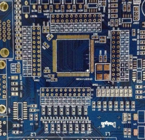
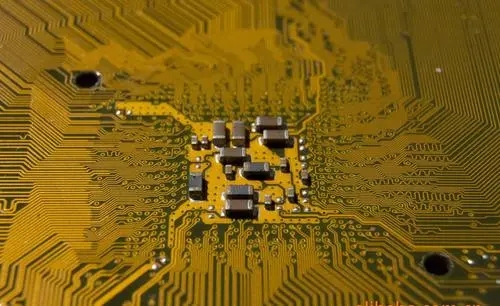
Circuit board

Skin effect: skin effect is a phenomenon that high-frequency components begin to approach the outside of the circuit board conductor rather than the inside. High frequency signals are also responsible for generating waveforms with different current values. Such signals have self inductance, which will increase with the increase of frequency. It is responsible for reducing the conductive area of the PCB surface, thus generating greater resistance and signal amplitude attenuation. Skin effect can be reduced by adding trace width (surface area), but this is not always feasible, because changing trace geometry may cause impedance problems.
As the signal range increases, so does the attenuation. The factors listed below are the causes of signal attenuation:
Noise source: RF frequency, leakage current and current interference cause signal attenuation. The greater the noise, the greater the attenuation!
Distance between transmitter and receiver: When the signal crosses a longer distance, its strength will decrease. The greater the distance between two points, the greater the attenuation.
Track width: the signal attenuates less when passing through a wider track.
Crosstalk: Crosstalk in nearby traces is also the cause of signal attenuation.
Conductor and connector: When the signal passes through different conductive materials and connector surfaces, the signal will be attenuated.
Transmission frequency: the shorter the wavelength, the greater the attenuation of radio wave. Such signals are transmitted by 2.4GHz or 5GHz electromagnetic waves. Electromagnetic waves have high frequency and short wavelength. In this case, the attenuation of wireless signal is very large, and it cannot be transmitted over a long distance.
Resistance loss related to conductor data: copper and other conductive data used in transmission line manufacturing will introduce resistance loss, resulting in attenuation of signals transmitted on copper trace lines.
Loss related to media data: The loss of media data sandwiched between transmission lines will lead to media loss. This dielectric loss forms conductance on the substrate, also known as reverse resistance, and absorbs part of the transmitted signal energy, leading to signal attenuation.
Copper surface roughness: The copper surface roughness on PCB will also hinder signal transmission. Rough copper wire will add resistance, because the terrain on the surface of the copper wire will cause the signal to move up and down. Surface spikes also add capacitance. Smooth copper is the solution to this problem, but the cost is higher.
Grounding circuit resistance: With the increase of frequency, the grounding circuit becomes narrower, and less copper area is used, resulting in the increase of resistance.
How to reduce signal attenuation?
The following technologies can reduce signal attenuation:
Use repeater: If the received signal is weak, use the repeater to regenerate the original signal by reducing attenuation. It also enhances the range of signals, which can be transmitted over longer distances without failure.
Use amplifier: If the received signal is weak, use the amplifier to increase its amplitude, which is different from the repeater that regenerates the whole signal.
Correct data selection: Careful selection of low loss dielectric materials and low resistance traces can minimize signal attenuation.
Use programmable differential output voltage (VOD) setting: The programmable VOD ensures that the drive strength is synchronized with the line impedance and PCB track length. The new driver's video on demand will enhance the receiver's signal.
Pre emphasis: Using amplifiers to enhance signal strength is not PCB signal attenuation control, because it will also amplify related signal noise and jitter Preemphasis enhances the high frequency component of the signal only by adding the level of the first transmission symbol If subsequent symbol levels are transmitted at the same level, they remain unchanged For example, if the signal transmits a high level of three symbols, only the first symbol is enhanced The next two symbols will be transmitted at the usual level
The above is the explanation given by the editor of pcb circuit board company.
If you want to know more about PCBA, you can go to our company's home page to learn about it.
In addition, our company also sells various circuit boards,
High frequency circuit board and SMT chip are waiting for your presence again.


Just upload Gerber files, BOM files and design files, and the KINGFORD team will provide a complete quotation within 24h.