
Professional PCB manufacturing and assembly
Building 6, Zone 3, Yuekang Road,Bao'an District, Shenzhen, China
+86-13410863085Mon.-Sat.08:00-20:00

Each person will probably have his own method to analyze the area estimation of the circuit board.
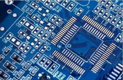
Circuit board design
For circuit board area estimation, you need to know some necessary coefficients.
1. Circuit board assembly coefficient
Assembly area n required for component assembly= Σ Element area × Assembly factor
Manual insertion: Plug in manually. At this time, you should take into account the space for finger movement.
2. Circuit coefficient
Factor for minimum line width and spacing. The larger the coefficient is, the larger the circuit board area is.
HV circuit coefficient=HV linewidth coefficient × High voltage line spacing coefficient
Low voltage circuit coefficient=signal linewidth coefficient × Power line width factor × GND line width coefficient × Low voltage line spacing coefficient
3. Layer coefficient
4. Calculation formula of PCB design area
Total assembly area of components=total assembly area of components in low-voltage area+total assembly area of components in high-voltage area
Total assembly area of components in low-voltage area=sum of assembly area of components in low-voltage area × Low voltage circuit coefficient.
Total assembly area of elements in high-voltage area=sum of assembly area of elements in high-voltage area × High voltage circuit coefficient.
Other areas
Designated prohibited area for final assembly
General assembly prohibited areas
Estimated area of circuit board=total assembly area of components × Layer coefficient+area of prohibited area for final assembly
Assembly limit coefficient=estimated area of circuit board/specified area of circuit board ≤ 1, usually less than 0.8. It is relatively easy to arrange component positions.
For specific examples, please refer to: Example of circuit board area estimation
1. PCB component assembly area
The calculation method of individual area of components is simply divided into rectangle and circle according to the projection of components on the circuit board.
x. Y represents the length and width of the rectangular element, respectively,
D is the diameter of the circular element
2. Circuit coefficient
Since only low voltage is involved here, the circuit coefficient is only 1.1025
3. Layer coefficient
Total assembly area of components × Layer coefficient=565 × one point one zero two five × 1 ≈ 630di
Generally, the prohibited area of the general assembly is estimated to be 684, (only when 630 is divided into 30mm × At 21mm, other splits will give different estimates.)
Add 3mm to the outside of each side, and the forbidden area of components. (36 × 27-630) × two
here × 2. Because both sides of the circuit board are set as component forbidden areas.
The estimated area of the circuit board is 1350 (round 1314) 1314=684+630
For the feasible area of circuit board design, the coefficient is 0.81350/0.8=1687.5 ≈ 1700mm2, which is relatively loose for this design. You can take it and fight with the product designer for a board with a length of 50mm and a width of 34mm. If the PCB product design does not allow it, you can only tighten your belt and set it to 0.9 or 1. If the coefficient of more than 1 is acceptable, it is also acceptable. It requires more effort and time on component positioning and PCB wiring.
In addition, according to the estimated area of the circuit board, check whether the circuit board size requirements given by the product circuit board designer are reasonable.


Just upload Gerber files, BOM files and design files, and the KINGFORD team will provide a complete quotation within 24h.