
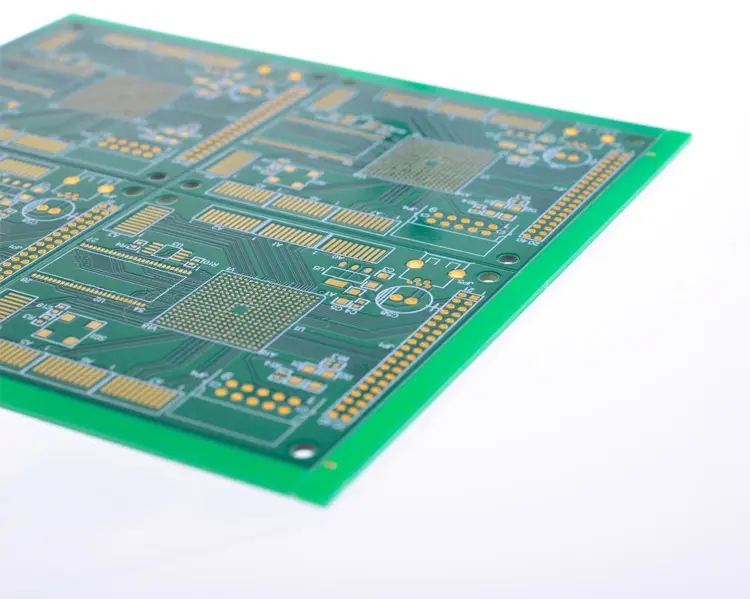
Professional PCB manufacturing and assembly
Building 6, Zone 3, Yuekang Road,Bao'an District, Shenzhen, China
+86-13410863085Mon.-Sat.08:00-20:00

The PCB design management system standardized by the professional team is strictly checked and comprehensively checked from schematic design, DFM, DFT, high-speed, EMC, thermal design, etc.
EMC refers to the ability of PCB equipment or system to operate in accordance with requirements in its electromagnetic environment and not produce unbearable electromagnetic interference to any equipment in its environment. On the one hand, reduce the emission of electromagnetic spectrum as much as possible, and on the other hand, protect the equipment from electromagnetic interference. Electromagnetic interference source, coupling path and receiver are the three elements to form interference, and the absence of any one of them will not form interference.
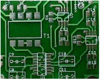
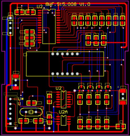
PCB design
Electromagnetic compatibility design is closely related to specific circuits. In order to conduct electromagnetic compatibility design, PCB design engineers need to minimize radiation (RF energy leaked from products) and enhance its susceptibility to radiation (energy entering products) and anti-interference capability. For the conductive coupling commonly seen at low frequencies and the radiation coupling commonly seen at high frequencies, cutting off the coupling path must be given full attention in PCB design. There are three basic principles for anti-interference design of PCB: PCB suppresses the interference source, cuts off the interference propagation path, and improves the anti-interference performance of sensitive devices.
1. PCB design suppresses interference sources
Suppressing interference sources is to reduce du/dt (digital device voltage change rate) and di/dt (digital device current change rate) of interference sources as much as possible. This is the most priority and most important principle in anti-interference design, which can often achieve twice the result with half the effort. The du/dt of the interference source is reduced mainly by paralleling capacitors at both ends of the interference source. The di/dt of the interference source is reduced by connecting the inductance or PCB resistance in series in the interference source circuit and adding a freewheeling diode.
2. Cut off the interference propagation path
(1) Fully consider the influence of power supply on PCB microcontroller. If the power supply is well done, the anti-interference of the whole circuit will be more than half solved. Many single chip computers are very sensitive to power supply noise. To reduce the interference of power supply noise to single chip computers, filter circuits or voltage regulators should be added to the power supply.
(2) Pay attention to crystal oscillator wiring. The crystal oscillator shall be as close as possible to the pin of the microcontroller, and the clock area shall be isolated by the ground wire. The crystal oscillator shell shall be grounded and fixed.
(3) The circuit board shall be reasonably partitioned, such as strong and weak signals, digital and analog signals. Try to keep the interference sources (such as motors and relays) away from the sensitive elements (such as SCM).
(4) The digital area shall be isolated from the analog area with a ground wire. The digital ground shall be separated from the analog ground, and finally connected to the power supply ground at one point. The wiring of A/D and D/A chips is also based on this principle.
3. Improve the anti-interference performance of sensitive devices in pcb design
Improving the anti-interference performance of sensitive devices refers to the method of minimizing the pickup of interference noise and recovering from abnormal state as soon as possible from the sensitive devices. Common measures to improve anti-interference performance of sensitive devices:
(1) For the idle I/O port of the microcontroller, do not hang in the air, but ground or connect to the power supply. The idle terminals of other ICs are grounded or connected to the power supply without changing the system logic.
(2) The use of power supply monitoring circuit for MCU can greatly improve the anti-interference performance of the entire PCB circuit.
(3) On the premise that the speed can meet the requirements, reduce the crystal frequency of the microcontroller as much as possible and select low-speed digital circuit.
(4) IC devices shall be directly welded to the circuit board as much as possible, and IC sockets shall be used less.


Just upload Gerber files, BOM files and design files, and the KINGFORD team will provide a complete quotation within 24h.