
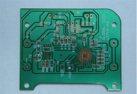
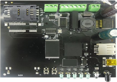
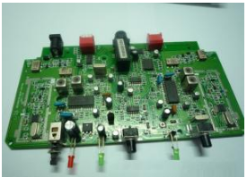
Professional PCB manufacturing and assembly
Building 6, Zone 3, Yuekang Road,Bao'an District, Shenzhen, China
+86-13410863085Mon.-Sat.08:00-20:00

In the assembly process of PCB devices, the wave soldering technology is generally selected for the welding of the pcb board components of the installation experience hole plug-in element (PTH). Wave soldering has many shortcomings: 1. It is not allowed to spread high density, thin spacing patch type components on the welding surface; 2. More bridging and false welding; 3. Welding fluid to be painted; Pcb board suffered from large thermal shock deformation.
Because the relative density of power circuit assembly is getting higher and higher at this stage, it is difficult to avoid that the welding surface may be covered with high-density, thin spacing patch type components. The traditional wave peak welding process has long been helpless for this matter. Generally, the only way to do this is to independently carry out flow back welding on the patch type components on the welding surface, and then manually fabricate welding to repair the remaining software spot welding, but there is a problem of poor consistency of spot welding quality. Four new types of hybrid welding technology are constantly emerging 01 Selectable welding Selectable welding, only some special areas touch the solder wire wave. Because PCB itself is a poor thermal conductivity material, it is not easy to heat up and melt the spot welding of adjacent electronic devices and PCB areas during welding. Before welding, it is also necessary to coat the soldering flux in advance. The soldering flux is only applied to the position to be welded under the PCB, but it can be selectively welded and should not be used to weld patch type components.
02. Immersion welding process shall be applied to select welding process, which can weld 0.7mm~11mm spot welding. The welding process of short leg position and small size welding layer is more stable, and the bridging probability is also small. The distance between adjacent spot welding edges and welding nozzles shall exceed mm. The following basic parameters can be applied to the selection of immersion welding process:
① Solder wire temperature 275 ℃~ 300 ℃
② Infiltration rate: 22mm/s~25mm/s
③ Infiltration time 1s~3s
④ Rate after immersion: 3mm/s
⑤ The speed of shock pump is determined by the total number of welding nozzles..
03. Through hole reflow (THR) of through-hole reflow soldering furnace is the application of reflow soldering technology to assemble through-hole components and special-shaped components. Because commodities pay more and more attention to practicality, lifting function and the relative density of lifting components, many single - and double-sided circuit boards are dominated by surface mounted components. However, due to the original compressive strength, reliability, versatility and other factors, the through-hole components are still superior to SMC in some cases, especially the RF connector at the edge of PCB. The disadvantage of using through-hole components on circuit boards dominated by surface mounted components is the high cost of spot welding alone. For such assembly lines, the key is to show the same reflow soldering furnace for through-hole and surface mounted components in the whole process of a single integrated PCB process.
Compared with the general surface mount process, the amount of solder paste used in the through-hole flow back process is 30 times more than that of the general SMT. At this stage, the through-hole flow back process selects two kinds of solder paste coating technologies, including solder paste packaging and printing and full-automatic solder paste spotting.
1. Solder paste packaging and printing. Steel mesh packaging printing is the preferred way to stack solder paste on PCB. The thickness of the steel mesh is an important factor, which will harm the solder paste amount on the missed PCB. Step steel mesh can be selected, which is specially designed for through-hole components in the thicker areas. This kind of screen design scheme can consider different solder paste quantity.
2. Fully automatic solder paste point. Fully automatic solder paste spotting has succeeded in stacking solder paste with proper volume for through-hole and special-shaped parts. It shows the coordination ability and working ability of many solder paste stacks that steel mesh packaging and printing will not be able to complete. When applying solder paste to the exposed Plated Through Hole (PTH), it is proposed to use a nozzle slightly larger than the diameter of PTH. In this way, when you spot the solder paste, force the solder paste to close to the hole edge of the PTH, squeeze the raw materials slightly from the bottom of the PTH, and then insert the parts from the reverse direction of the solder paste. If a nozzle with a diameter smaller than PTH is used, the solder paste will be discharged from the hole and cause serious solder paste damage.
The through-hole reflow soldering furnace can replace the wave soldering machine at many levels to complete the welding of plug-in components, especially in solving the welding of software spot welding with high-density patch type components (or with thin spacing SMD) on the welding surface, which greatly improves the welding quality, which can fill in the shortage of expensive machinery and equipment. The appearance of through-hole reflow soldering furnace has greatly helped to enrich the welding methods, improve the relative density of pcb pcb assembly, improve the welding quality and reduce the process steps.
PCBA
04. The application of shielded mold wave soldering technology is technical. Because the traditional wave soldering technology can not solve the welding of patch type components with fine spacing and high density on the welding surface, a new way came into being: the shielded mold mask patch type components were used to complete the wave soldering of the plug-in wires on the butt welding surface.
1. The application of shielding off the advantages of mold wave soldering technicality 1) completes the production and manufacturing of dual mixed PCB wave soldering machine, which can greatly improve the productivity of dual mixed PCB and prevent the problem of poor quality consistency existing in manual manufacturing and welding. 2) Reduce the advance preparation time for sticking solder mask, improve productivity and reduce product cost. 3) The production is equal to the traditional wave crest welding machine.
2. Shielding the raw materials of the mold 1) The mold must be anti-static, and the common raw materials are: aluminum alloy profiles, synthetic stone, plywood. When using synthetic stone, it is proposed not to use gray black synthetic stone to prevent the wave crest welder controller from non magnetic induction. 2) The die plate is thin and thick. According to the thickness of the components on the back of the machine disk, select the plate with a thickness of mm~8mm to make the mold.
3. Mold process specification
1) Dimension of the mold: the length and width of the mold are respectively equivalent to the length and width of the PCB plus the total width of the mobile carrier side of 60mm, and the total width of the mold must be ≤ 350mm. When the total width of PCB is less than 14b250m, it can be considered to place two additional PCBs in one mold for welding.
2) The process edge is 8mm away from the edge. In addition, 11 mm wide and 11 mm high bakelite boards are refitted near the edge on both sides to improve the compressive strength of the mold and reduce mold deformation.
3) Each lifting bar must be fixed with screws, and the space between the screws shall be less than 150mm.
4) After the mold is made, press buckles (fixed PCB on the mold) need to be installed around and within 100 mm interval, and the following contents must be noted: ① Do not touch the parts after rotating for one week; ② No harm to DIP software; ③ The PCB can be fastened to the mold.
5) Four corners of the die shall be provided with a R5 fillet.
6) When PCBA on the mold passes through the tin furnace, some parts will float due to the impact of tin wave, so some parts that are easy to float will be treated by pressing. Key methods selected at this stage:
① Metal material wood block pressing piece;
② Install press fasteners on the mold;
③ Make anti floating high pressure fixture. Summary The technicality of the welding process to be selected depends on the characteristics of the goods: if the goods are large in quantity and small in variety, the technicality of the selective drag welding process can be taken into account, without making professional molds, but the investment in machinery and equipment projects is large. If PCB products are single in variety, large in batch, and want to adapt to the traditional wave soldering process, consider the application of shielded mold wave soldering technology, but the project must invest in making professional molds. These two welding technical processes are easy to operate, so Shengde is widely used in the assembly production of electronic components at this stage. Through hole flow back welding is a very promising welding method because of its high process manipulation difficulty coefficient and less relativity. However, it is very helpful to improve welding quality, enrich welding methods and reduce PCB process steps.


Just upload Gerber files, BOM files and design files, and the KINGFORD team will provide a complete quotation within 24h.