
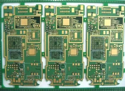
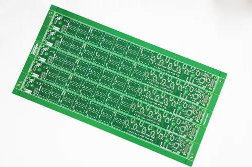
Professional PCB manufacturing and assembly
Building 6, Zone 3, Yuekang Road,Bao'an District, Shenzhen, China
+86-13410863085Mon.-Sat.08:00-20:00

Flexible smart driver makes PCB layout more orderly
The flexible smart driver PCB board layout is more orderly. Small flexible electronic systems, such as mobile phones, PMP (personal media player), DSC (digital camera), DVC (digital camera), PME (portable medical equipment) and GPS (positioning system), have been developing continuously. Their functional characteristics exceed those of the next generation Therefore, the requirements of some peripheral circuits are often similar, because their power supply, port, and MMI (human machine interface) all use similar technologies
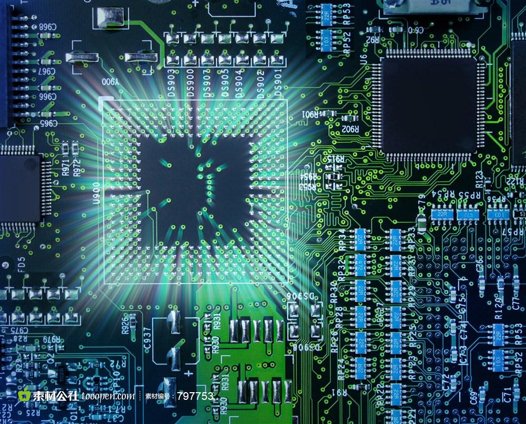
PCB board

Three-level strategy for low-power full-function products
With the increase of functions and performance of portable systems, the demand for power management is also increasing Therefore, the strategies used by OEMs to solve power consumption problems are evolving The first level strategy focuses on the efficiency of the energy management subsystem, including minimizing DC losses/DC converters, LDO, battery management, and battery protection circuits This is a power subsystem centric approach, which largely depends on the ability of transistor suppliers to produce components and integrated devices that consume less power than devices with similar architectures on the market This makes OEM engineers' main task is to select components, balance energy efficiency, component cost, and package size Although this strategy works well, the component market has also realized its benefits. Most analog and analog mixed signal IC suppliers have not benefited greatly from the reduced process size
The focus of the second level of compliance is shifted from power supply to some parts of the system, even if some parts of a large AS or C do not work at a specific time This strategy is particularly effective when it is applied to high power users such as wireless connection hardware and display backlight, and can extend the working time of each charge, I/O port, or nonvolatile memory allocation by turning off low power loads such as audio subsystem Today's mobile phones, for example, have 20 or more power zones In addition to saving idle current in high-power circuits such as RF components and display backlights, this strategy can effectively reduce static power consumption as long as the system can turn off the clock drive part of the circuit With the development of IC manufacturing technology to smaller size, this strategy can effectively replace clock gating to reduce no-load current This energy-saving strategy depends on the technical contributions of the system architect, hardware and software implementers, and ASIC suppliers Although this strategy is successful, it is also limited by the load on the application processor. These additional functions force designers to consume more and more powerful computing resources For example, mobile phones have been transferred from ARM7 to ARM9 and ARM11 processors as optional baseband and secondary processing resources Similar trends have emerged in other portable electronic products, although to a lesser extent
The third level strategy focuses on reducing the power consumption of various functions without sacrificing performance One possible technology is to use distributed intelligent management, which does not require strong processing power and speed of baseband or application processors This strategy allows the processor to transfer all functions to the semi-automatic peripheral controller As a result, the processor can enter the sleep mode during human activities, instead of data processing or communication tasks that require the full power of the processor, such as the backlight driver of the intelligent display screen
Backlight scheme under the third level strategy
Users of portable electronics require a screen display that is clearly visible in all ambient light conditions. The current portable devices usually use photodiodes or transistors to estimate the ambient light intensity and use it as the input of backlight driver control A photosensitive sensor requires a signal conditioning circuit: a DC biased form of excitation, amplification and A/D conversion or at least one or two threshold detection levels Through external components or analog I/O chip pins, the main processor usually monitors the output of the photosensitive sensor in the form of periodic data conversion The speed of this conversion varies from one to several orders of magnitude per second Then, the controller evaluates the results and generally divides them into three categories, one for each day, for well lit indoor environments or for poorly lit environments The processor does this by sending a control signal to the backlight driver, which provides one of three possible current levels for the LED string But this is not efficient Effective, this is a way to manage microprocessors: delegate tasks to a part of the system at a low running cost under the supervision of powerful and expensive central resources This does not seem to help with processor task offloading
1. Intelligent driver transfers processor tasks
Solutions based on the ADP5520 smart Backlight driver derive significant energy savings from LED drivers that can operate under microcontroller configuration control or automatically manage display lighting. The ADP5520 consists of an asynchronous boost converter, a programmable ambient light management circuit, a state machine, and a configurable port extender to further save system resources The boost converter can supply power for up to six white LEDs in series, with a series voltage of up to 24.5V and a drive current of up to 30mA The ambient light measurement unit is divided into an ambient light sensor to provide all signal adjustment functions. Together with the on-chip state machine and the boost converter, 128 current levels from 0 to 30 mA are realized The ADP5520 was able to increase the operating time per charge by 15% in tests simulating variant mobile phone usage (Figure 1) Adding ambient light detection to the ADP5520 control method resulted in 50% more standby time per charge than the baseline measurement These curves are analogous to mobile interactive applications that do not require RF functionality, such as games, text and email reading and writing, or camera applications Designers hope that their products can smoothly transition between different light levels, not just switch The lighting scheme under the control of the processor requires a lot of processor interaction to achieve smooth transition. In addition, compared with simple switch control, it significantly increases the load of the processor Smart LED driver, such as ADP5520, can realize various lighting and darkening current changes, including linear, square, and cubic laws, thus further reducing processor load (Figure 2) This configurable driver has 15 discontinuous and independent fade out times, ranging from 300ms to 5.5 seconds There is a resettable dimming timer on the chip, which can be programmed as one of 15 time intervals from 10 seconds to 120 seconds
2. Smart drives provide additional low-bandwidth capabilities
In addition to saving energy, such smart drives can provide more value by supporting other low-frequency wide peripheral devices For example, the ADP5520 integrates a configurable port extender that provides eight I/O pins The two I/O pins can also be connected to the third dedicated pin as independent current absorption pins, switching, and flash control for LED indicators with programmable dimming Other pins can be programmed for keyboard or general I/O These auxiliary LED drivers consume 0 to 14 mA of current and can be dimmed or dimmed in 64 steps As with the main backlight current consumption, the indicator connected to the auxiliary driver pin can be turned on or off, or light adjustment can be achieved through a linear or nonlinear sequence
3. The intelligent driver can reduce the number of PCB cables
To allow configuration data to flow from the processor to the smart drive and for status, I/O or keystroke data flows back to the processor. The ADP5520 implements an I2C interface This setting reduces the number of devices and wires between peripheral devices and controllers, thus simplifying the design of high-density PCB electronic devices


Just upload Gerber files, BOM files and design files, and the KINGFORD team will provide a complete quotation within 24h.