
Professional PCB manufacturing and assembly
Building 6, Zone 3, Yuekang Road,Bao'an District, Shenzhen, China
+86-13410863085Mon.-Sat.08:00-20:00

The following is an introduction to the concept and significance of PCB layer in PCB design
1、 Top layer and bottom pad layer of PCB board layer:
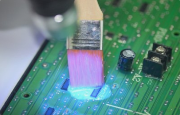
Toppaste and bottompaste are the top and bottom pad layers, which refer to the copper and platinum exposed outside, (For example, we draw a wire on the top wiring layer. What we see on the PCB is just a wire, which is covered by the whole green oil. But we draw a square or a dot on the toppass layer at the position of the wire. The square and the dot on the printed board have no green oil, but copper platinum.

Topsolder and bottomsolder are just the opposite of the previous two layers. It can be said that these two layers are the layers to be covered with green oil, In fact, if the solder layer is not added to the wiring after wiring, the green oil will be added by default when it is made at the pcb manufacturer. If the solder layer is added, the exposed copper foil will be seen here after the pcb is made. It can be understood as mirror phase.
2、 The paste layer is used when making the steel mesh before the pcb patch. It is used to coat solder paste. The electronic components of the patch are pasted on the solder paste for reflow soldering. The differences between DrillGuide and DrillDrawing are: 1. DrillGuide is used to guide drilling, and C8051 chip decryption is mainly used for manual drilling to locate. 2. DrillDrawing is used to view the hole diameter. When manually drilling, these two files should be used together. But now most of them are CNC drilling, so these two layers are not very useful. When positioning holes are placed, it is not necessary to place content on these two layers. Just place vias and pads with corresponding apertures on the Mechanical or TOPLAYER or bottomlayer layers. Do not place the diameter smaller. As for the two layers of Mechanical and MultiLayer, they are as follows: 1. Mechanical is a mechanical layer, which is used to place mechanical graphics, such as the shape of a PCB. 2. MultiLayer can be called a multi-layer. The graphics placed on this layer have corresponding graphics on any layer, and the keepout layer that will not be screen printed with solder resist is not actually used to draw the shape of a PCB. The real purpose of keepout layer is to prohibit wiring, That is to say, after placing graphics on the keepout layer, there will be no corresponding graphic copper foil at the corresponding positions on the wiring layer (such as toplayer and bottomlayer), and all wiring layers. This does not happen after placing drawings on the Mechanical layer.
3、 The mechanical layer defines the appearance of the entire PCB. In fact, when we say the mechanical layer, we mean the appearance structure of the entire PCB. The forbidden wiring layer is the boundary of the copper layer that defines the electrical characteristics of our wiring. That is to say, after we first define the forbidden wiring layer, the wires with electrical characteristics that we lay in the subsequent wiring process cannot exceed the boundary of the forbidden wiring layer. Top overlay and bottom overlay are silk screen characters that define the top and bottom layers. They are component numbers and some characters that we usually see on PCB boards. Toppaste and bottompaste are the top and bottom pad layers, which refer to the copper and platinum exposed outside, (For example, we draw a wire on the top wiring layer. What we see on the PCB is just a wire, which is covered by the whole green oil. But we draw a square or a dot on the toppass layer at the position of the wire. The square and the dot on the board are free of green oil, but copper platinum. The top and bottom layers are just opposite to the previous two layers, which can be as follows That said, these two layers are the layers to be covered with green oil. The multilaye layer is actually similar to the mechanical layer. Gu Ming Enyi, this layer refers to all layers of the PCB.
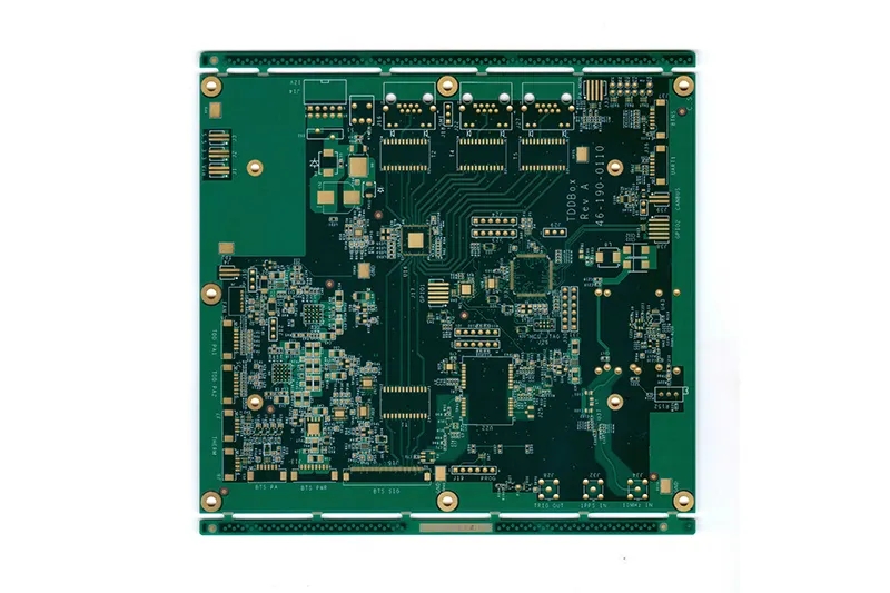
1. The concept of "layer" is similar to the concept of "layer" introduced in word processing or many other software to realize the nesting and composition of drawings, texts, colors, etc. Protel's "layer" is not virtual, but the actual copper foil layers of the printed board material itself. Nowadays, the components of electronic circuits are installed intensively. With special requirements such as anti-interference and wiring, PCB printed boards used in some newer electronic products not only have upper and lower sides for wiring, but also have sandwich copper foils that can be specially processed in the middle of the board. For example, the printed board materials used in today's computer motherboards are more than four layers. Because it is relatively difficult to process these layers, most of them are used to set power wiring layers with simple routing (such as Ground Developer and Power Developer in the software), and they are usually wired by means of large area filling (such as ExternaI P1a11e and Fill in the software). The places where the upper and lower surface layers need to be connected with the middle layers are communicated by the so-called "Via" mentioned in the software. With the above explanation, it is not difficult to understand the concepts of "multi-layer pad" and "wiring layer setup". To take a simple example, many people have completed wiring and found that many connected terminals do not have pads until printing. In fact, this is because they ignored the concept of "layers" when adding device libraries and did not define the characteristics of the pads they drew and packaged as "Mulii Layer". It should be noted that once the number of layers of the printed board used is selected, you must close those unused layers to avoid causing trouble and making mistakes.


Just upload Gerber files, BOM files and design files, and the KINGFORD team will provide a complete quotation within 24h.