
Professional PCB manufacturing and assembly
Building 6, Zone 3, Yuekang Road,Bao'an District, Shenzhen, China
+86-13410863085Mon.-Sat.08:00-20:00


PCB board test and design program
With the increasing miniaturization, PCB board components and wiring technology have also made great progress. For example, highly integrated micro integrated circuits packaged in BGA housings have reduced the insulation distance between wires to 0.5mm, for example The wiring design method of electronic components has more and more influence on whether the test can be carried out smoothly in the future production process Here are some important rules and useful tips Following some programs (DFT design for testability, design for testability) can greatly reduce the cost of preparing and implementing production tests These programs have been developed over the years. Of course, if new production and component technologies are introduced, they must be expanded and adjusted accordingly With the structure of electronic products becoming smaller and smaller, there are two outstanding problems: first, fewer and fewer circuit nodes can be contacted; Another reason is that methods such as online testing applications are limited In order to solve these problems, corresponding measures can be taken in circuit layout, and new test methods and innovative adapter solutions can be used The solution to the second problem also involves generating additional tasks for the test system that was originally used as an independent trip These tasks include programming memory components through the test system, or implementing self-test of integrated components (including self-test, BIST, and built-in self-test). Transfer these steps to the test system to create more added value in general In order to successfully implement these measures, corresponding factors must be considered in the product development stage
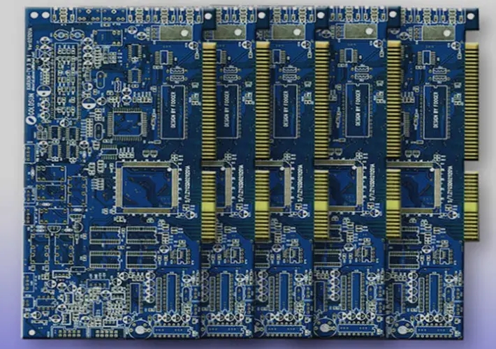
PCB board

1. What is testability
The meaning of testability can be understood as: test engineers can use the simplest method to check the characteristics of a component to see whether it can meet the expected functions. In short:
How easy is it to test whether the product meets the technical specifications?
How fast can you write a test program?
How comprehensive is the discovery of product failures?
How easy is it to access test points?
In order to achieve good testability, mechanical and electrical design practices must be considered. Of course, there is a cost to achieve testability, but it has a series of benefits for the whole process. In conclusion, it is an important prerequisite for successful product production.
2. Why to develop and test friendly technology
In the past, if the product could not be tested at the previous test point, the problem would only be pushed to one test point. If product defects cannot be found during production testing, it is only necessary to transfer the identification and diagnosis of defects to functional and system testing. On the contrary, today people try to find defects as early as possible. The advantage is not only that the cost is low, but also that today's products are very complex, and some manufacturing defects may not be detected in functional testing. For example, for some components to be pre installed with software or programming, this problem exists. (such as flash memory or ISP: programmable device in the system). The programming of these components must be planned at the development stage, and the test system must master the programming. Test friendly circuit design requires some money, however, test difficult circuit design requires more money. Testing itself has costs, which increase with the increase of test series; From online testing to functional testing and system testing, testing costs are increasing. Skipping one of these tests will cost more. The general rule is to increase the cost of each test by 10 times. Through test friendly circuit design, faults can be detected early, so as to quickly compensate the funds spent on test friendly circuit design.
How files affect testability
Only by making full use of the complete data in component development can we develop a test program that can completely detect failures. In many cases, close cooperation between development and testing is necessary. Archives have an indisputable influence on test engineers' understanding of component functions and developing test strategies. To avoid problems caused by lack of files and insufficient understanding of component functions, test system manufacturers can rely on software tools that automatically generate test patterns on a random basis, or rely on non vector methods, which can only be considered as a stopgap measure. The complete file before the test includes parts list, circuit design data (mainly CAD data) and detailed information about the functions of service components (such as data sheet). With all the information, you can compile test vectors, define component failure modes, or perform some pre adjustments. Some mechanical data are also important, such as the data required to check whether the components are well welded and aligned. For programmable components, such as flash memory, PLD, FPGA, etc., if they are not programmed during installation, they should be programmed on the test system, and their programming data must also be known. The programming data of flash memory device shall be complete. If the flash memory chip contains 16Mbit data, it should be able to use 16Mbit, which can prevent misunderstanding and avoid addressing conflicts. For example, this may happen if you use 4Mbit memory to provide only 300Kbit data to the component. Of course, the data should be prepared in a popular standard format, such as Intel's hexadecimal or Motorola's s record structure. Most test systems can interpret these formats as long as they can program flash or ISP components. Many of the information mentioned above is also necessary for component manufacturing. Of course, manufacturability and testability should be clearly distinguished, because they are completely different concepts, which constitute different premises.
4. Mechanical contact conditions with good testability
Even if the circuit has good electrical testability, it is difficult to test without considering the basic rules of mechanics. Many factors limit the power testability. If the test points are not enough or too small, it is difficult for the probe base adapter to reach each node of the circuit. If the position error and size error of the test point are too large, the test repeatability will be poor. When using a probe bed adapter, follow a series of recommendations regarding the size and location of keyholes and test points.
5. Electrical prerequisites for testability
Both electrical prerequisites and mechanical contact conditions are essential for good testability. The grid circuit cannot be tested. The reason may be that the starting input terminal cannot be contacted through the test point, or the starting input terminal is in the package and cannot be contacted from the outside. In principle, neither situation is good. Make the test impossible. When designing circuits, it should be noted that all components tested by the on-line test method should have some mechanism to enable each component to be electrically isolated. This mechanism can be achieved by disabling the input, which controls the output of the component in the static high ohm state. Although almost all test systems can reverse drive the node state to any state, the involved nodes still need to be equipped with a disable input. First, make the node in a high ohm state, and then "gently" add the corresponding level. Similarly, the beat generator is always disconnected directly from the back of the oscillator through the starting lead, grid or plug-in bridge. The start input should not be connected directly to the circuit, but should be connected to the circuit through a 100 ohm resistor. Each component should have its own start, reset or control pin. It must be avoided that the start inputs of many components share a resistor connected to the circuit. This rule also applies to ASIC components, which should also have a lead pin through which the output can be brought to a high ohm state. If it is possible to reset the components when the operating voltage is turned on, the tester start reset is also useful. In this case, you can simply put the component in the specified state before testing. Unused component wires should also be accessible, because short circuits not found in these places may also cause component failures. In addition, unused gates are usually used for design improvement in the future and can be re wired into the circuit. Therefore, it is also important to test it from the beginning to ensure the reliability of its workpiece.
The above is the explanation given by the editor of pcb circuit board company. If you want to know more about PCBA, you can go to our company's home page to learn about it. In addition, our company also sells various circuit boards,
High frequency circuit board and SMT chip are waiting for your presence again.
What is AOI automatic optical detector?
Nov 04,2022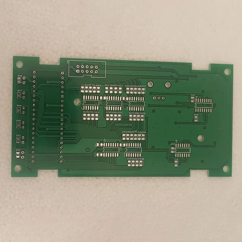


Just upload Gerber files, BOM files and design files, and the KINGFORD team will provide a complete quotation within 24h.