
Professional PCB manufacturing and assembly
Building 6, Zone 3, Yuekang Road,Bao'an District, Shenzhen, China
+86-13410863085Mon.-Sat.08:00-20:00


Parasitic capacitance and inductance of PCB through hole
1. Passed
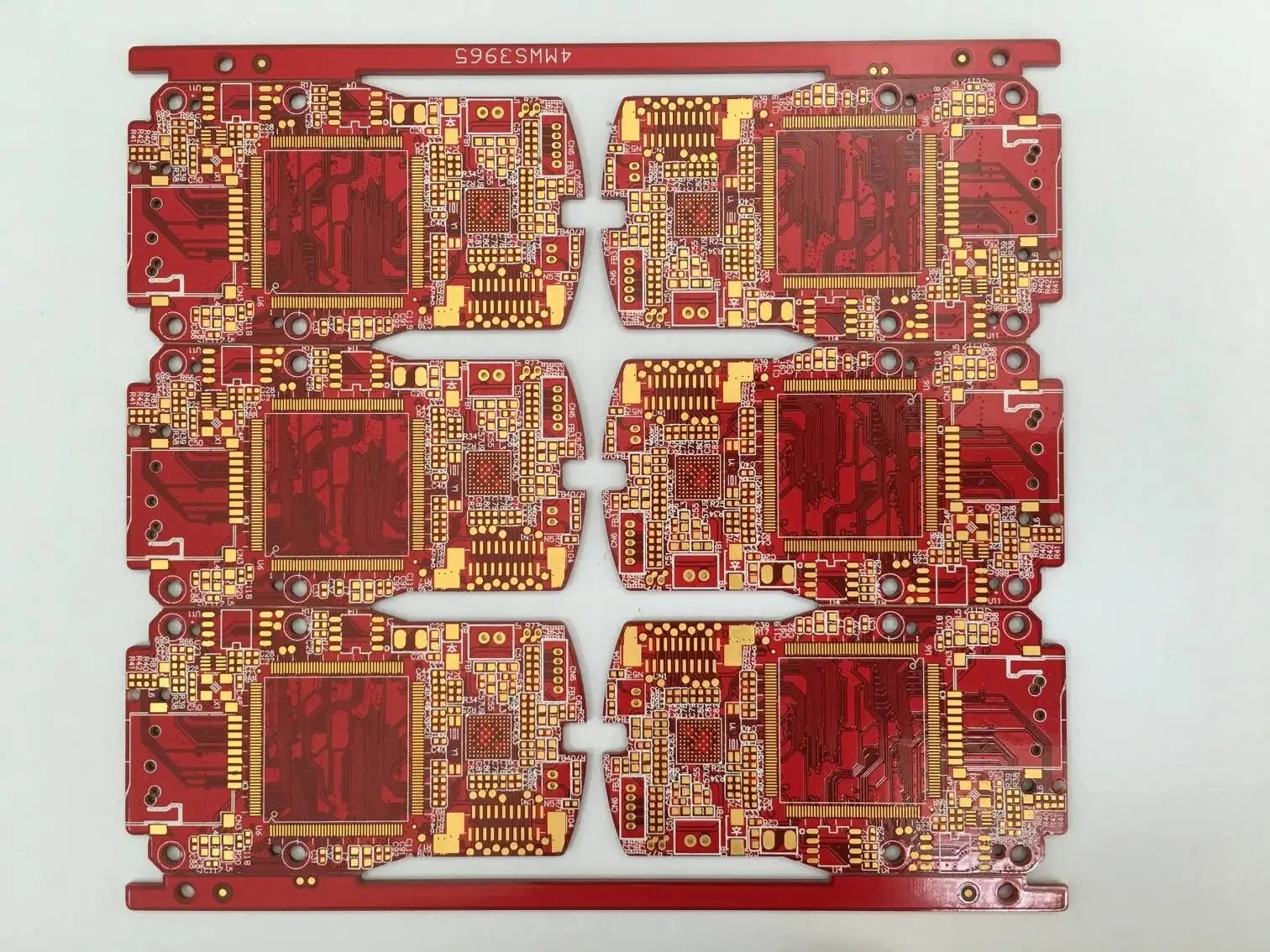
Through hole is one of the important components of multilayer structure PCB board, and the drilling cost usually accounts for 30% to 4.0% of the drilling cost In short, each hole on a PCB can be called a through-hole From the functional point of view, through holes can be divided into two categories: one is used for electrical connection between layers; The other is used for equipment fixation or positioning In terms of process, these through-holes are generally divided into three categories: blind through-hole, embedded through-hole, and through through-hole The blind hole is located on the top and bottom of the printed circuit board, with a certain depth, and the depth of the hole usually does not exceed a certain ratio (diameter) Embedded through-hole refers to the connection hole located in the inner layer of the printed circuit board, which does not extend to the surface of the circuit board The above two types of holes are located in the inner layer of the circuit board and are completed by the through hole forming process before lamination During the formation of the through-hole, several inner layers may overlap The third type is called through hole, which runs through the whole circuit board and can be used for internal interconnection or as the mounting position hole of components Because through-hole is easier to realize in process and lower in cost, most printed circuit boards use it to replace the other two kinds of through-hole Unless otherwise specified, the following through holes are considered as through holes From the design point of view, vias are mainly composed of two parts: one is the middle hole, and the other is the pad area around the hole, as shown in the following figure: The size of these two parts determines the size of the through-hole Obviously, in the high-speed and high-density design of PCB boards, designers always hope that the smaller the through-hole is, the better, so as to leave more wiring space on the circuit board In addition, the smaller the through-hole is, the larger its parasitic capacitance is, and the smaller it is, the more suitable it is for high-speed circuits However, the reduction of the hole size also brings new costs, and the size of the through hole cannot be infinitely reduced It is limited by drilling and electroplating technology: the smaller the hole, the longer the training time The longer the time is, the easier it is to deviate from the center position; When the depth of the hole is more than 6 times of the drilling diameter, uniform copper plating on the hole wall cannot be guaranteed For example, the normal 6-layer thickness of PCB (through hole depth) is about 50Mil. After all, the hole diameter is very small by the PCB manufacturer, and can only reach 8 mil
2. Parasitic capacitance of through-hole
The hole itself has parasitic capacitance to ground. If it is known that the diameter of the isolation hole of the through-hole on the ground plane is D2, the diameter of the through-hole pad is D1, the thickness of the PCB is T, the dielectric constant of the board substrate is Q µ, and the parasitic capacitance of the through-hole is similar to: C=1.41 μ。 For example, for a PCB with a thickness of 50Mil, if a through-hole with an inner diameter of 10Mil and a pad diameter of 20Mil is used, and the distance between the pad and the copper grounding area is 32Mil, the through-hole can be approximated by the above formula. Parasitic capacitance is approximately: C=1.41x4.4 × 0.050 × 0.020/(0.032-00200)=0.517pF, and the rise time change caused by this part of capacitance is: T10-90=2.2C (Z0/2)=2.2 × 0.517 x (55/2)=31.28ps. From these values, it can be seen that although the effect of slow rise caused by parasitic capacitance of a single through-hole is not obvious, the designer should carefully consider whether the through-hole is used to switch between layers in the trace for many times.
3. Through hole parasitic inductance
Similarly, the parasitic inductance exists together with the parasitic capacitance of the through-hole. In the design of high-speed digital circuits, the harm caused by parasitic inductance through the hole is often greater than that caused by parasitic capacitance. Its parasitic series inductance will weaken the contribution of bypass capacitors and reduce the filtering effect of the entire power system. The diameter of the through-hole has little influence on the inductance, while the length of the through-hole has a great influence on the inductance. Using the above example, the inductance of the through-hole can be calculated as: L=5.08x0.050 [ln (4x0.05/0.010) 1]=1.015nH. If the rise time of the signal is 1ns, its equivalent impedance is XL=Ï L/T10-90=3.19 Î L. When high frequency current passes through, this impedance can no longer be ignored. When connecting the power supply layer and the ground plane, the bypass capacitor needs to pass through two through holes, thus doubling the parasitic inductance of the through holes.
4. Through hole design on high-speed PCB

Through the above analysis of via parasitic characteristics, we can see that in the design of high-speed PCB boards, seemingly simple via often brings great negative effects to circuit design. To reduce the adverse effects caused by via parasitic effects, you can try to:
1) Considering the cost and signal quality, the through-hole with reasonable size is selected. For example, for a 6-10 layer storage module PCB design, it is best to use 10/20Mil (drill/pad) through-hole. For some high-density small circuit boards, you can also try to use 8/18 million. Through hole. Under the current technical conditions, it is difficult to use smaller through holes. For power or ground through-hole, consider using a larger size to reduce impedance.
2) From the two formulas discussed above, it can be concluded that using thinner PCB is beneficial to reduce the two parasitic parameters of through holes.
3) Try not to change the layer of signal trace on PCB, that is, try not to use unnecessary through-hole.
4) The pins for power and ground should be as close to the drill hole as possible. The leads between the through-hole and the pin should be as short as possible because they add inductance. At the same time, the power and ground leads should be as thick as possible to reduce impedance.
5) Place some ground through-hole near the via where the signal changes layers to provide a close return path for the signal It can even be used in a large number of PCB boards Of course, flexibility is also required in the design The through-hole model discussed above is the case that each layer has pads. Sometimes, we can reduce or even remove pads from some layers Especially in the case of very high through-hole density, this may lead to the formation of circuit breakers on the copper layer To solve this problem, in addition to moving the position of the through-hole, we can also consider moving the through-hole on the copper layer of PCB Reduced pad size
14 Common Errors in PCB Design for Engineers
Nov 03,2022


Just upload Gerber files, BOM files and design files, and the KINGFORD team will provide a complete quotation within 24h.