
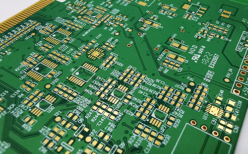
Professional PCB manufacturing and assembly
Building 6, Zone 3, Yuekang Road,Bao'an District, Shenzhen, China
+86-13410863085Mon.-Sat.08:00-20:00

Selection of Microwave PCB Substrate
For the selection of alternatives to microwave PCB, the dielectric efficiency should be considered first, but at the same time, the type and thickness of copper foil surface, environmental adaptability, processability, other factors, and cost must be considered
Type and thickness of copper foil The substitute for microwave PCB is 35 Î ¼ M and 18 Î; ¼ M Two The thinner the copper foil is, the easier it is to obtain high graphic accuracy. This high-precision microwave graphic should not exceed 18 ° C ¼ M Copper foil If 35 inch is selected ¼ M Copper foil, high graphic accuracy makes the machinability worse, and the proportion of unqualified products will inevitably increase IPCB's microwave PCB manufacturing experience believes that the type of copper foil will also affect the accuracy of graphics At present, there are two types of copper foil: calendered copper foil and electrolytic copper foil The calendered copper foil is more suitable for manufacturing high-precision graphics than electrolytic copper foil, so when selecting microwave PCB data, you can consider selecting the base material plate of the calendered copper foil
Machinability Selection of Microwave PCB Alternatives With the continuous improvement of design requirements, some microwave PCB substrates are equipped with aluminum gaskets. The appearance of this aluminum lining substrate brings additional pressure to the manufacturing process. The graphic production process is complex, the contour processing is complex, and the production cycle is extended. This, no matter whether it is available or not, the base material with aluminum liner shall not be used as much as possible.
Rogers TMM series microwave substrate is composed of thermosetting resin filled ceramic powder. Among them, TMM10 substrate is filled with more ceramic powder, which is fragile in efficiency, brings great difficulties to pattern manufacturing and contour processing, and is easy to damage or form internal cracks, with relatively low yield. At present, the laser cutting method is used to process the shape of TMM10 sheet, which has high cost, low efficiency and long production cycle. Remember, if possible, RT/Daroid series substrates of Rogers Company can be selected to meet the corresponding dielectric efficiency requirements.
The environmental adaptability of alternatives to microwave PCB circuit boards There is no problem that the existing microwave substrate is within the environmental temperature range required by the - 55 –+125 – standard. But there are two things to consider,
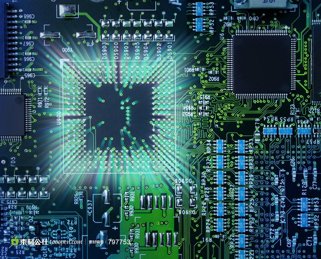
Mm PCB

1. Effect of porosity on substrate selection. For microwave plates that need through hole metallization, the greater the Z-axis thermal expansion coefficient of the substrate, which means that the greater the possibility of metallized hole fracture under high temperature and low temperature impact. In this case, on the premise of meeting the dielectric efficiency, the substrate with smaller thermal expansion coefficient of Z-axis should be selected as far as possible
2. The influence of humidity on the selection of substrate: the water absorption of the substrate resin itself is very small, but after adding the enhancement data, the overall water absorption will increase, and the use in a high humidity environment will affect the dielectric efficiency. In this case, the base material with low water absorption shall be selected, or structural and technological measures shall be taken to protect it.
Structural Design Microwave PCB is more and more complex due to the appearance of microwave board, and requires high dimensional accuracy The output of the same variety is large, so it is necessary to apply CNC milling technology Therefore, when designing the microwave board, the characteristics of NC processing should be fully considered. The internal corners of all processing parts should be designed as rounded corners to facilitate one-time processing and molding
The structural design of microwave board should not pursue too high accuracy, because the dimensional deformation trend of non-metallic materials is large, and the machining accuracy of metal parts cannot be used to require microwave board. The high accuracy requirement of the profile may be that when the microstrip line is connected to the profile, the profile deviation will affect the length of the microstrip line, thus affecting the microwave efficiency. In fact, a gap of 0.2mm should be left between the end of the microstrip line and the edge of the plate to avoid the influence of contour processing deviation.
Microwave PCB manufacturing technology is different from ordinary single-sided, double-sided and multilayer boards. It not only acts as a structural component and connector, but also acts as a signal transmission line. The manufacturing of microwave is limited by the following factors: the number of microwave manufacturing layers, the characteristics of microwave raw materials, the requirements for metalized hole manufacturing, the final surface coating method, the characteristics of circuit design, the accuracy requirements of manufacturing lines, the advancement of manufacturing equipment and liquid drugs, and the manufacturing technology will be adjusted accordingly according to specific requirements. For example, the circuit nickel gold plating process is divided into graphic nickel gold positive film process and graphic nickel gold negative film process. According to different microwave types and processing requirements, different manufacturing technologies are adopted,
Microwave PCB Process Description
1. When the circuit graphics are interconnected, the negative process of nickel gold plating for graphics can be selected
2) In order to improve the qualification rate of microwave manufacturing, the negative printing process of pattern nickel gold electroplating should be adopted as far as possible. Because if the positive plate process of graphic nickel gold electroplating is adopted, if the operation is not properly controlled, the quality problem of nickel gold penetration will occur
3) ROGERS microwave plate of RT/duroid 6010 base plate brand will be scrapped due to long hair at the edge of the line during pattern electroplating after etching, so the positive plate process of pattern nickel plating must be adopted
4) When the manufacturing accuracy of the circuit is required to be within ± 0.02mm, the corresponding point of each process must adopt the wet film plate making process
5) When the manufacturing accuracy of the circuit is required to be greater than ± 0.03mm, the dry film or wet film plate making process can be used in the corresponding part of each process
6. For PTFE dielectric microwave plates, such as ROGERS RT/duroid 5880, RT/Duroid 5870, ULTRALAM2000, RT/Duroid 6010, etc., sodium naphthalene solution or plasma can be used for hole metallization. However, TMM10, TMM10i, RO4003, RO4350, etc. do not require activation pretreatment.
Manufacturing of microwave PCB is developing towards the common rigid process of FR-4. More and more rigid manufacturing technologies and technologies are applied to microwave processing It is embodied in the multi-layer structure of microwave manufacturing, the improvement of circuit manufacturing accuracy, the three-dimensional NC machining and the diversification of surface coatings In addition, with the further addition of microwave PCB substrate types and the continuous improvement of design requirements, PCBA needs to further optimize the existing microwave manufacturing technology and keep pace with the times to meet the growing microwave demand for PCB manufacturing
PCB board design and signal integrity analysis
Oct 27,2022


Just upload Gerber files, BOM files and design files, and the KINGFORD team will provide a complete quotation within 24h.