
Professional PCB manufacturing and assembly
Building 6, Zone 3, Yuekang Road,Bao'an District, Shenzhen, China
+86-13410863085Mon.-Sat.08:00-20:00


How to handle PCB board signal crossing the boundary
In PCB design, the division of power plane or grounding plane will lead to incomplete plane, so that when signal is routed, its reference plane will be displayed from one power plane to another, This phenomenon is called signal cross segmentation For low-speed signals, cross segmentation may not matter, but in high-speed digital signal systems, high-speed signals use the reference plane as the return path, which is the return path When the reference plane is incomplete, the following adverse effects will occur: it will cause discontinuous impedance of the trajectory; It is easy to cause crosstalk between signals; It will cause reflection between signals; New current loop area and new loop inductance make the output waveform easy to oscillate; The newly added radiation interference to space is easily affected by space magnetic field; The possibility of magnetic field coupling with other circuits on the circuit board is added; High frequency voltage drop on loop inductance. It forms a common mode radiation source and generates common mode radiation through external cables Therefore, PCB wiring should be as close to the plane as possible to avoid cross splitting These conditions are only allowed when the low-speed signal line must be separated or cannot be close to the power ground plane
PCB board
1. Treatment of cross segmentation in design
If cross segmentation is unavoidable in PCB design, how to deal with it? In this case, the segmentation needs to be repaired to provide a short return path for the signal. Common treatment methods include adding patch capacitors and jumper bridging.
2. Suture capacitor
Typically, 0402 or 0603 encapsulated ceramic capacitors are placed on the signal cross section. The capacitance of the capacitor is 0.01 uF or 0.1 uF. If space allows, you can add multiple such capacitors. At the same time, try to ensure that the signal line is within 200 mils of the sewing capacitor, and the smaller the distance is, the better; The network at both ends of the capacitor corresponds to the reference plane network through which the signal passes. See the network connected at both ends of the capacitor in the figure below. The two colors are highlighted. Two different networks:
3. Cross line bridging
Usually, the signal layer "packs the ground" for cross segmented signals, and may also include signal lines of other networks. This "packet" line should be as thick as possible.
4. Multilayer wiring
High speed signal wiring circuit usually has high integration and high wire density. The use of multilayer boards is not only necessary for wiring, but also an effective means to reduce interference. Reasonable selection of the number of layers can greatly reduce the size of the printed circuit board, make full use of the middle layer to set the mask, better realize the nearby grounding, effectively reduce the parasitic inductance, effectively shorten the signal transmission length, and greatly reduce the signal cross interference.
5. The less the lead wire bends, the better
Lead wire bending between pins of high-speed circuit equipment shall be as small as possible. The leads of high-speed signal wiring circuit are straight lines and need to be rotated. They can be rotated with 45 ° polylines or arcs. This requirement is only used to improve the fixing strength of steel plates in low-frequency circuits. In high-speed circuits, meeting this requirement can reduce the external emission and mutual coupling of high-speed signals, and reduce the radiation and reflection of signals.
6. The shorter the lead, the better
The wiring between pins of high-speed signal wiring circuit device shall be as short as possible. The longer the wire, the greater the distributed inductance and capacitance, which will have a great impact on the passing of high-frequency signals in the system, and will also change the characteristic impedance of the circuit, leading to system reflection and oscillation.
7. The less alternating between lead layers, the better
The less alternating between lead layers between pins of high-speed circuit equipment, the better. The so-called "less interlaminar alternating of the leads, the better" means that the fewer through holes used in the component connection process, the better. According to the measurement, a through-hole can bring about about 0.5 pf of distributed capacitance, which leads to a significant increase in circuit delay. Reducing the number of vias can significantly improve the speed

8. Beware of parallel cross interference
In high-speed signal wiring, attention should be paid to the "cross interference" introduced by parallel wiring of adjacent signal lines. If parallel distribution cannot be avoided, a large area of "grounding" can be arranged opposite the parallel signal line to greatly reduce interference.
9. Avoid branches and stumps
High speed signal routing shall avoid branches or stubs as much as possible. Stubs have a great impact on impedance and may cause signal reflection and overshoot, so we should generally avoid stubs and branches in design. Use chrysanthemum cables to reduce the impact on the signal.
10. The signal line should be as far away as possible in the inner layer
High frequency signal lines are prone to generate large electromagnetic radiation on the surface, and are also vulnerable to external electromagnetic radiation or interference factors High frequency signal lines are routed between the power supply and the ground wire. The absorption of electromagnetic waves by the power supply and the bottom layer will greatly reduce the radiation generated by the PCB board

Layout and wiring principle of RF PCB
Oct 27,2022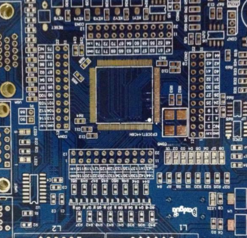


Just upload Gerber files, BOM files and design files, and the KINGFORD team will provide a complete quotation within 24h.