

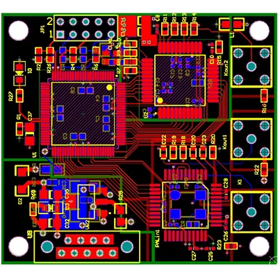
Network equipment circuit board design
Name: Network equipment circuit board design
Designable layers: 1-32 layers
Minimum line width and line spacing: 3mil
Minimum laser aperture: 4mil
Minimum mechanical aperture: 8mil
Copper foil thickness: 18-175цm (standard: 18цm35цm70цm)
Peel strength: 1.25N/mm
Minimum punching hole diameter: single side: 0.9mm/35mil
Minimum hole diameter: 0.25mm/10mil
Aperture tolerance: ≤φ0.8mm±0.05mm
Hole tolerance: ±0.05mm
Hole wall copper thickness: double-sided/multi-layer: ≥2um/0.8mil
Hole resistance: double-sided/multi-layer: ≤300цΩ
Minimum line width: 0.127mm/5mil
Minimum pitch: 0.127mm/5mil
Screen printing color: black, white, red, green, etc.
Surface treatment: lead/lead-free tin spray, ENIG, silver, OSP
Service: Provide OEM service
Certificate: ISO9001.ROSH.UL
The names of circuit boards are: ceramic circuit board, alumina ceramic circuit board, aluminum nitride ceramic circuit board, circuit board, PCB board, aluminum substrate, high frequency board, thick copper board, impedance board, PCB, ultra-thin circuit board, ultra-thin circuit board Thin circuit boards, printed (copper etching technology) circuit boards, etc. The circuit board makes the circuit miniaturized and intuitive, and plays an important role in the mass production of fixed circuits and the optimization of the layout of electrical appliances. Circuit boards can be called printed circuit boards or printed circuit boards, FPC circuit boards (FPC circuit boards, also known as flexible circuit boards, flexible circuit boards are a kind of high reliability made of polyimide or polyester film as the base material. , an excellent flexible printed circuit board. It has the characteristics of high wiring density, light weight, thin thickness and good bendability.) and the birth and development of the flexible and rigid combination board-FPC and PCB, gave birth to the combination of flexible and rigid board this new product. Therefore, the soft-rigid board is a circuit board with FPC characteristics and PCB characteristics formed by combining flexible circuit boards and rigid circuit boards according to relevant process requirements through lamination and other processes.
Name: Network equipment circuit board design
Designable layers: 1-32 layers
Minimum line width and line spacing: 3mil
Minimum laser aperture: 4mil
Minimum mechanical aperture: 8mil
Copper foil thickness: 18-175цm (standard: 18цm35цm70цm)
Peel strength: 1.25N/mm
Minimum punching hole diameter: single side: 0.9mm/35mil
Minimum hole diameter: 0.25mm/10mil
Aperture tolerance: ≤φ0.8mm±0.05mm
Hole tolerance: ±0.05mm
Hole wall copper thickness: double-sided/multi-layer: ≥2um/0.8mil
Hole resistance: double-sided/multi-layer: ≤300цΩ
Minimum line width: 0.127mm/5mil
Minimum pitch: 0.127mm/5mil
Screen printing color: black, white, red, green, etc.
Surface treatment: lead/lead-free tin spray, ENIG, silver, OSP
Service: Provide OEM service
Certificate: ISO9001.ROSH.UL
