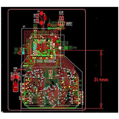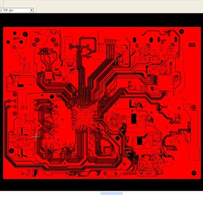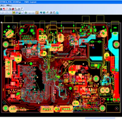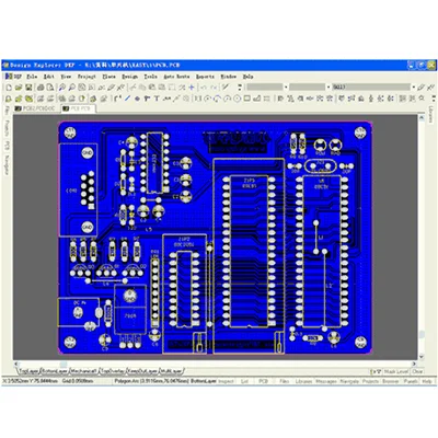
PCB design of fast charging power bank
Name: PCB design of fast charging power bank
Designable layers: 1-32 layers
Minimum line width and line spacing: 3mil
Minimum laser aperture: 4mil
Minimum mechanical aperture: 8mil
Copper foil thickness: 18-175цm (standard: 18цm35цm70цm)
Peel strength: 1.25N/mm
Minimum punching hole diameter: single side: 0.9mm/35mil
Minimum hole diameter: 0.25mm/10mil
Aperture tolerance: ≤φ0.8mm±0.05mm
Hole tolerance: ±0.05mm
Hole wall copper thickness: double-sided/multi-layer: ≥2um/0.8mil
Hole resistance: double-sided/multi-layer: ≤300цΩ
Minimum line width: 0.127mm/5mil
Minimum pitch: 0.127mm/5mil
Screen printing color: black, white, red, green, etc.
Surface treatment: lead/lead-free tin spray, ENIG, silver, OSP
Service: Provide OEM service
Certificate: ISO9001.ROSH.UL
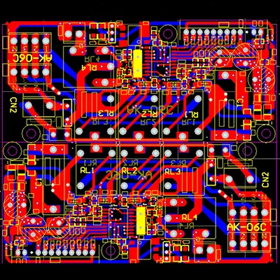
What is a power bank circuit board?
The charging and discharging module integrates the microusb interface, and the mobile power circuit board can be used to charge other electronic products. The power bank circuit board integrates overcurrent protection, overvoltage protection and undervoltage protection. The power bank has high precision.
fast charging for short
Fast charging refers to a charging method that can make the battery reach or close to a fully charged state within 1 to 2 hours.
Name: PCB design of fast charging power bank
Designable layers: 1-32 layers
Minimum line width and line spacing: 3mil
Minimum laser aperture: 4mil
Minimum mechanical aperture: 8mil
Copper foil thickness: 18-175цm (standard: 18цm35цm70цm)
Peel strength: 1.25N/mm
Minimum punching hole diameter: single side: 0.9mm/35mil
Minimum hole diameter: 0.25mm/10mil
Aperture tolerance: ≤φ0.8mm±0.05mm
Hole tolerance: ±0.05mm
Hole wall copper thickness: double-sided/multi-layer: ≥2um/0.8mil
Hole resistance: double-sided/multi-layer: ≤300цΩ
Minimum line width: 0.127mm/5mil
Minimum pitch: 0.127mm/5mil
Screen printing color: black, white, red, green, etc.
Surface treatment: lead/lead-free tin spray, ENIG, silver, OSP
Service: Provide OEM service
Certificate: ISO9001.ROSH.UL
- Previous:GPS Base Station PCB/PCBA Design
- Next:sphygmomanometer PCB design