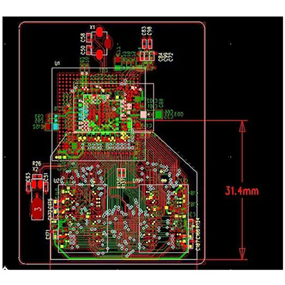
RF equipment PCB/PCBA design
Name: RF equipment PCB/PCBA design
Designable layers: 1-32 layers
Minimum line width and line spacing: 3mil
Minimum laser aperture: 4mil
Minimum mechanical aperture: 8mil
Copper foil thickness: 18-175цm (standard: 18цm35цm70цm)
Peel strength: 1.25N/mm
Minimum punching hole diameter: single side: 0.9mm/35mil
Minimum hole diameter: 0.25mm/10mil
Aperture tolerance: ≤φ0.8mm±0.05mm
Hole tolerance: ±0.05mm
Hole wall copper thickness: double-sided/multi-layer: ≥2um/0.8mil
Hole resistance: double-sided/multi-layer: ≤300цΩ
Minimum line width: 0.127mm/5mil
Minimum pitch: 0.127mm/5mil
Screen printing color: black, white, red, green, etc.
Surface treatment: lead/lead-free tin spray, ENIG, silver, OSP
Service: Provide OEM service
Certificate: ISO9001.ROSH.UL
1. Introduction to RF PCB Design
In the wireless communication system, only a small part of the front-end circuit works in the radio frequency stage, which is commonly known as the radio frequency front-end circuit. The rest of the circuit is used for low frequency baseband analog and digital signal processing. RF front-end circuits generally include low-noise amplifiers, mixers and power amplifiers. Although the number of components in this part of the circuit is much less than that of the baseband circuit, it is still the key to the success or failure of the entire system.
Similar to the octagon rule for analog IC design, RF PCB design requires analog signal processing at wide dynamic range and high frequencies. Therefore, RF PCB design also has its own hexagon rule. Noise, linearity, supply voltage, gain, operating frequency and power are the most important metrics in an RF PCB. In practical designs, any two or more of these parameters will constrain each other, resulting in multidimensional optimization problems. Such compromises and mutual constraints bring many problems to the design of RF PCBs. Often it takes the intuition and experience of the RF designer to arrive at a better compromise.
Second, the application field of RF PCB
(1) Base station RF circuit board
(2) Mobile phone RF circuit board
(3) Wireless Local Area Network (WLAN) RF PCB
(4) Global Positioning System (GPS) RF circuit board
(5) Radio Frequency Tag (RFID) RF PCB
(6) Internet of Things (IOT) RF PCB
Name: RF equipment PCB/PCBA design
Designable layers: 1-32 layers
Minimum line width and line spacing: 3mil
Minimum laser aperture: 4mil
Minimum mechanical aperture: 8mil
Copper foil thickness: 18-175цm (standard: 18цm35цm70цm)
Peel strength: 1.25N/mm
Minimum punching hole diameter: single side: 0.9mm/35mil
Minimum hole diameter: 0.25mm/10mil
Aperture tolerance: ≤φ0.8mm±0.05mm
Hole tolerance: ±0.05mm
Hole wall copper thickness: double-sided/multi-layer: ≥2um/0.8mil
Hole resistance: double-sided/multi-layer: ≤300цΩ
Minimum line width: 0.127mm/5mil
Minimum pitch: 0.127mm/5mil
Screen printing color: black, white, red, green, etc.
Surface treatment: lead/lead-free tin spray, ENIG, silver, OSP
Service: Provide OEM service
Certificate: ISO9001.ROSH.UL
- Previous:No
- Next:GPS Base Station PCB/PCBA Design


