

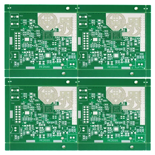
Hybrid high frequency PCB board
Name: Hybrid high frequency PCB board
Material: Rogers4835+IT180A
Layers: 6L
Copper Thickness: 1oz
Plate thickness: 1.2mm
Minimum aperture: 0.15mm
Minimum line spacing: 0.1mm
Minimum line width: 0.1mm
Surface Treatment: Immersion Gold
Hybrid PCBs are commonly used in microwave RF series products
With the rapid development of electronic communication technology, in order to achieve high-speed, high-fidelity signal transmission, more and more microwave RF PCBs are used in communication equipment. Dielectric materials for high-frequency hybrid circuit boards have excellent electrical properties and good chemical stability, mainly in the following four aspects.
1. Hybrid PCB has the characteristics of small signal transmission loss, short transmission delay time, and small signal transmission distortion.
2. Excellent dielectric properties (mainly refers to low relative dielectric constant DK, low dielectric loss factor DF). In addition, the dielectric properties (DK, DF) remain stable under environmental changes such as frequency, humidity and temperature.
3. High-precision characteristic impedance control.
4. Hybrid PCB has excellent heat resistance (TG), processability and adaptability.
Microwave high frequency hybrid PCB is widely used in wireless antennas, base station receiving antennas, power amplifiers, radar systems, navigation systems and other communication equipment.
Based on one or more factors such as cost savings, increased flexural strength, and control of electromagnetic interference, high-frequency lamination designs must use high-frequency prepregs with low resin flow and FR-4 substrates with smooth dielectric surfaces. Frequency composite laminate. In this case, there is a great risk in the adhesion control of the product during pressing.
Microwave high-frequency hybrid PCB stacking method and characteristics
1. A high-frequency hybrid PCB controlled depth composite laminate structure, the high-frequency hybrid PCB includes L1 copper layer (high frequency sheet), L2 copper layer (PP sheet), L3 copper layer (epoxy resin substrate), L4 in order Copper layer; slot holes of the same size are set in the same position of L2, L3, L4 copper layer; L4 copper layer is arranged with three-in-one buffer material from inside to outside, steel plate and kraft paper are stacked from outside to outside in turn; aluminum plate, steel plate, Kraft paper is stacked on the L1 copper layer from inside to outside.
2. According to the first feature, the three-in-one buffer material is a buffer material sandwiched between two release films.
3. According to the first feature, the laminated structure of the high-frequency plate-controlled deep-mixing plate of the present invention is characterized in that the high-frequency sheet is a polytetrafluoroethylene plate.
The expansion and contraction characteristics of high-frequency hybrid PCB composite laminates are different from ordinary epoxy resin substrates, so the curvature and shrinkage of the board are difficult to control, and the processing method of first slotting and then pressing will cause the problem of sheet metal dents. The three-in-one buffer material is arranged on one side of the groove, and the buffer material can be filled into the groove hole during pressing, so as to avoid the problem of depression. Kraft paper is set on both sides of the cardboard to buffer pressure and balance heat transfer evenly, and steel plates are set to ensure uniform heat conduction during pressing, so that the pressing is flat, and the heat and pressure during the pressing process are balanced, so as to better control the curvature and expansion of the board.
With the rapid development of 5G communication technology, higher frequency requirements for communication equipment are required. There are a variety of microwave high frequency hybrid PCBs on the market. The manufacturing technology of these microwave high-frequency hybrid PCBs also puts forward higher requirements. Professional processing iPCB for more than 10 years, can provide multi-layer hybrid PCB manufacturing services, has all the equipment required for the whole process of multi-layer hybrid PCB production, in line with ISO9001-2000 international standardized management system, and has passed iatf16949 and ISO 14001 system certification. Its products are UL certified and comply with IPC-A-600G and IPC-6012A standards. Can provide high-quality, high-stability, high-adaptability microwave high-frequency hybrid PCB samples and batch services.
Name: Hybrid high frequency PCB board
Material: Rogers4835+IT180A
Layers: 6L
Copper Thickness: 1oz
Plate thickness: 1.2mm
Minimum aperture: 0.15mm
Minimum line spacing: 0.1mm
Minimum line width: 0.1mm
Surface Treatment: Immersion Gold
