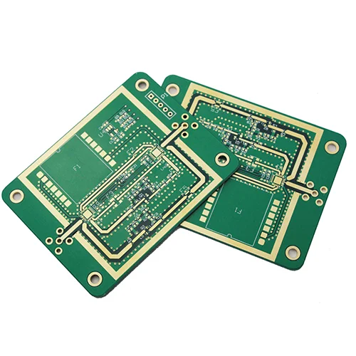
Isola high frequency board
Name: Isola high frequency board
Layers: 4L
Plate thickness: 1.0mm
Plate used: Isola high frequency plate
Size: 76.3mm*69.9mm
Z small aperture: 0.25mm
Dielectric constant: 3.38
Layer: 2L
Substrate thickness: 0.813mm (32mil)
Product thickness: 0.9mm
Copper Plating Thickness: 1 oz (35μm)
Surface Treatment: Immersion Gold
Minimum line width/line spacing: 6mil/6mil
application:
Automotive, Backplane, RF/Microwave, High-End Computing
Signal Integrity, Medical, Military, Mobile Devices/Wireless Handsets
Railroads, Servers, Switches/Routers, Thermal Management, Wireless Infrastructure
What does Isola PCB mean?
Such printed circuit boards are complex and manufactured using high performance laminates. It incorporates resin components designed to meet demanding performance requirements.
This type of PCB is used in most electronic devices, such as aerospace equipment and high-end consumer electronics.
Types of materials used in Isola PCBs
There are materials used to make Isola PCBs. Some of these include
Prepreg
The term is associated with the PCB industry. It's called "pre-dipping". This is a dielectric material that provides electrical insulation as well as other important functions. It is made through a fiberglass fabric infused with a uniquely formulated resin.
The resin combines different thermal, electrical and physical properties with the prepreg. This is important to correct the operation of Isola PCB.
CCL
This consists of a prepreg laminate with a thin layer of copper foil on both ends. This lamination is achieved by compressing one or more layers of copper and prepreg together under extreme heat, pressure and vacuum conditions.
Building Multilayer Isola PCBs
Prepreg and CCL are used to fabricate multilayer Isola PCBs through complex operations involving multiple processes that are often repeated.
The copper surface of the laminate is etched. This is for the production of electronic circuits. Next, the laminates are assembled by inserting one or more layers of prepreg between each etched laminate to form a multilayer structure.
Electroplating and drilling then form electrical interconnects between the PCB layers. The resulting Isola PCB is an interconnect gadget in which semiconductors and other components are mounted.
Isola PCB Applications
Isola PCB's laminates and prepregs are used in different devices and advanced electronics, including:
Aerospace applications
Military electronic applications
Industrial equipment applications
High-end consumer electronics
Network and other communication equipment
Automotive applications
Medical device applications
What materials are used in Isola PCB's resin systems?
Isola PCB uses no-flow prepregs, which are polyimide-based for PCB applications that require high temperatures.
They use a polyimide flame retardant resin system and are ideal for applications requiring superior performance and thermal performance. Isola's prepregs feature polyimide blends and thermoplastic resins that fully cure without the use of methylene diphenylamine (MDA).
This then results in a polymer with a high Tg, which does not have the problems of brittleness and low initial bond strength. Therefore, the resin system of Isola PCB is much better than the resin structure of traditional thermosetting polyimide.
Features of Isola Prepregs
Here are some key features of Isola PCB materials:
Maintains bond strength at elevated temperatures
Halogen-free option available
Higher thermal performance
Reduces delamination due to machining
Enhanced workability due to reduced brittleness
Long service life of resin system
Name: Isola high frequency board
Layers: 4L
Plate thickness: 1.0mm
Plate used: Isola high frequency plate
Size: 76.3mm*69.9mm
Z small aperture: 0.25mm
Dielectric constant: 3.38
Layer: 2L
Substrate thickness: 0.813mm (32mil)
Product thickness: 0.9mm
Copper Plating Thickness: 1 oz (35μm)
Surface Treatment: Immersion Gold
Minimum line width/line spacing: 6mil/6mil