
Professional PCB manufacturing and assembly
Building 6, Zone 3, Yuekang Road,Bao'an District, Shenzhen, China
+86-13410863085Mon.-Sat.08:00-20:00

The so-called copper pouring is to use the unused space as the reference surface and then fill it with solid copper. These copper areas are also called copper pouring areas. The significance of copper plating is to reduce the impedance of ground wire and improve the anti-interference ability; Reduce the voltage drop and improve the efficiency of the power supply; Connecting to a ground wire can also reduce the loop area. In addition, most people also need to fill the opening area of the PCB with copper wire or grid ground wire in order to keep the PCB from deforming as much as possible during PCB welding. If copper is handled improperly, there will be no return or loss. Is Copper Plating "More Advantages Than Disadvantages" or "More Disadvantages Than Advantages"
Use the EMSCAN EMI scanning system to obtain the following measurements. EMSCAN enables us to view the distribution of electromagnetic fields in real time. It has 1218 near-field probes and uses electronic switch technology to scan the electromagnetic field generated by PCB at high speed. It is the only electromagnetic field near-field scanning system in the world using array pcb antenna and electronic scanning technology, and the only system that can obtain complete electromagnetic field information of the measured object.
Let's look at a practical case. On the multilayer , thePCB engineer places a circle of copper around the PCB, as shown in Figure 1. In this copper coating process, the engineer placed only a few through holes at the beginning of the copper shell and connected the copper shell to the ground plane. There is no through hole in other places.
Electromagnetic field with frequency of 22.894Mhz generated by PCB with poor grounding
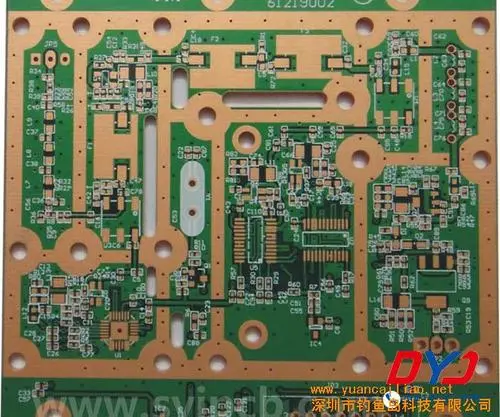
Circuit board
At high frequency, the distributed capacitance of printed pcb wiring will play a role. When the length is greater than 1/20 of the wavelength corresponding to the noise frequency, the antenna effect will be generated, and the noise will be emitted through the wiring.
From the above actual measurement results, there is a 22.894MHz interference source on the PCB. The copper plate is very sensitive to this signal, and the signal is received as a "receiving antenna". At the same time, copper plates are also used as "transmitting antennas". The "antenna" emits strong electromagnetic interference signals to the outside.
The relationship between frequency and wavelength is f=C/ λ。
In the formula, f is the frequency in Hz, λ Is the wavelength, in m; C is the speed of light, equal to 3 * 108 m/s. For 22.894MHz signal, its wavelength λ It is: 3 * 108/22.894M=13m. λ/ 20 is 65cm.
The copper wire of this PCB is too long, more than 65cm, causing antenna effect.
At present, in our PCB, we usually use chips with rising edges less than 1ns. Assuming that the rising edge of the chip is 1ns, the frequency of electromagnetic interference generated by the chip will be as high as fknee = 0.5/Tr = 500MHz. For a 500MHz signal, the wavelength is 60cm, λ/ 20=3cm。 In other words, 3 cm long wiring on the PCB can form an "antenna".
Therefore, in high-frequency circuits, do not think that if you ground somewhere, this is "ground". Make sure that holes are punched in the wiring and the spacing is less than λ/ 20, so as to be "well grounded" with the grounding plane of the multilayer board.
For general digital circuits, at a distance of 1cm to 2cm, the "grounding filling" on the element surface or welding surface is perforated to achieve a good grounding with the grounding plane, so as to ensure that the "grounding" will not produce a "bad" effect.
Therefore, the following extensions are made:
Do not use copper in the open area of the middle layer of the multilayer pcb. Because it's hard for you to make this copper "well grounded"
No matter how many power supplies are on the PCB, it is recommended to use power division technology and only use one power layer. Since the power supply is the same as the ground, it is also a "reference plane". The "good grounding" between the power supply and the grounding is achieved by a large number of filter capacitors. If there is no filter capacitor, there is no "grounding".
Metal inside the equipment, such as metal radiator and metal reinforcing strip, must be "well grounded".
Heat dissipation metal block of three terminal regulator


Just upload Gerber files, BOM files and design files, and the KINGFORD team will provide a complete quotation within 24h.