
Professional PCB manufacturing and assembly
Building 6, Zone 3, Yuekang Road,Bao'an District, Shenzhen, China
+86-13410863085Mon.-Sat.08:00-20:00

A single-sided paper substrate with a large number of holes and complex shapes and an epoxy glass cloth substrate with double-sided nonmetallic holes.
Stamping: mass production. Usually one or more sets of dies are used for stamping.
Shape processing: pcb printed boards produce a large number of single-sided and double-sided shapes, usually using dies. According to the size of pcb, it can be divided into upper blanking die and blanking die.
Composite processing: holes and holes of printed circuit boards, as well as holes and shapes, require high precision. At the same time, in order to shorten the manufacturing cycle and improve the productivity, composite dies are used to simultaneously process the holes and shapes of the veneer. The key to using mold to process PCB is mold design and processing, which requires professional technical knowledge. In addition, the mold installation and debugging are also very important. At present, most molds of PCB manufacturers are processed by external factories.
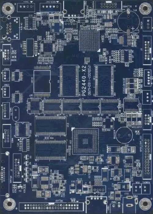
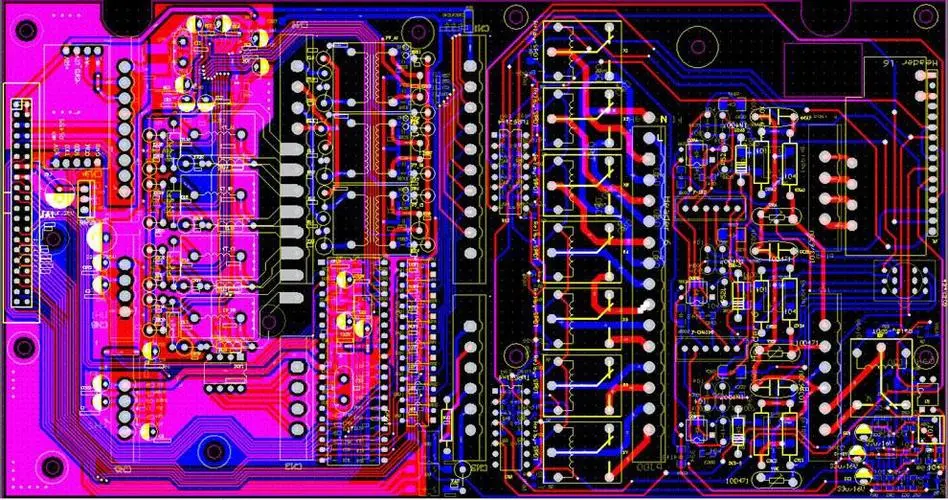
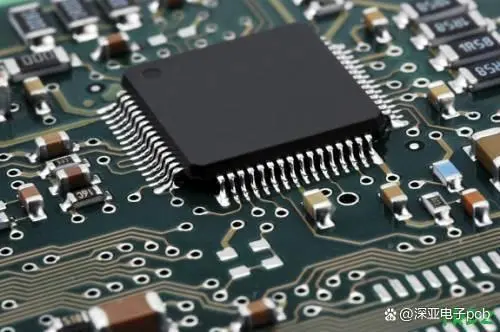
Circuit board

Precautions for mold installation:
Select punch (including type and tonnage) according to punching force, die size, closing height, etc. calculated by die design.
Open the punch, and comprehensively check whether the clutch, brake, slider and other components are normal, whether the operating mechanism is reliable, and whether there is no continuous punching.
The gasket under the mold is usually 2 pieces, which must be ground on the grinder at the same time to ensure that the mold is installed in parallel and vertical. The jumping position of the gasket will not hinder the blanking, and it should be as close to the center of the mold as possible.
Several sets of pressure plate and T-head pressure plate screws shall be prepared for use with the die. The front end of the pressing plate shall not contact the straight wall of the lower die. An emery cloth should be placed between the contact surfaces and the screws tightened.
When installing the mold, pay special attention to the screws and nuts on the lower mold, and do not contact the upper mold (the upper mold is lowered and closed)
When adjusting the mold, use manual instead of manual as far as possible.
In order to improve the stamping performance of the substrate, the paper substrate must be preheated. The temperature is preferably 70-90 ° C.
The quality defects of the hole and shape of the printed pcb circuit board punched by the die are as follows: the periphery of the hole is raised or the copper foil is warped or laminated; Cracks exist between holes; The hole position is not vertical or the hole body is not vertical; Large burr; Rough section; The perforated printed circuit board is bent into the shape of the tank bottom; Scrap jumps up; Waste is blocked. The inspection and analysis steps are as follows: check whether the punch force and rigidity are sufficient; Whether the die design is reasonable and the rigidity is sufficient; Whether the machining accuracy of punch and die, guide pillar and guide sleeve are concentric and vertical. Check whether the fit clearance is even. If the gap between the convex and concave is too small or too large, quality defects will occur, which is the most important problem in mold design, processing, debugging and use. The edges of punch and die shall not be rounded or chamfered. The punch is not allowed to have taper, especially when punching, whether it is positive taper or reverse taper. In the pcb production process, pay attention to whether the cutting edges of the male die and female die are worn. Whether the discharge outlet is reasonable and the resistance is small. Whether the push plate and punch are reasonable and the force is sufficient. When analyzing the stamping quality defects, the thickness of the sheet to be stamped, the adhesive force of the substrate, the amount of glue, the adhesive force with the copper foil, and the preheating humidity and time should also be considered.
Punch method and PCB blanking can be used for hole and shape processing. Blanking can be used for PCB boards with simple process or those with low requirements. It is applicable to the production of PCB with low requirements, low level and large capacity, as well as low shape requirements, with low cost.
last:


Just upload Gerber files, BOM files and design files, and the KINGFORD team will provide a complete quotation within 24h.