
Professional PCB manufacturing and assembly
Building 6, Zone 3, Yuekang Road,Bao'an District, Shenzhen, China
+86-13410863085Mon.-Sat.08:00-20:00


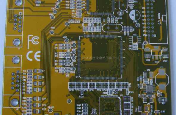
In the rapid development of science and technology today, a variety of high-tech electronic products emerge in an endless stream, which makes the demand for printed circuit boards increase sharply, manufacturing difficulties are becoming higher and higher, and quality requirements are becoming more and more stringent. In order to ensure the high quality and high stability of the printed circuit board, to achieve the total quality management of the PCB factory and the control of the environment, it is necessary to fully understand the characteristics of the printed circuit board manufacturing technology. However, printed circuit board manufacturing technology is a comprehensive technical crystallization, which involves the basic knowledge of physics, chemistry, optics, photochemistry, polymers, fluid mechanics, chemical dynamics and many other aspects, such as the structure, composition and performance of the material: the precision, stability, efficiency and processing quality of the process equipment; Feasibility of the process method; The accuracy and high reliability of detection means and the temperature, humidity, cleanliness and other problems in the environment. These problems will directly and indirectly affect the quality of PCB. Because there are many aspects and problems involved, it is easy to produce all kinds of quality defects. Therefore, it is necessary to carefully understand the quality problems that are most likely to occur and occur in each process, and quickly take technological measures to eliminate them and improve the production efficiency of PCB. We hereby collect, summarize and sort out the relevant materials for your enjoyment. Here, let's talk about the PCB substrate:

(1) the size of the substrate changes due to the difference in longitude and latitude directions; Because the fiber direction is not paid attention to during shearing, the shear stress remains in the substrate, and once released, it directly affects the shrinkage of the substrate size. Solution: Determine the law of change in the direction of longitude and latitude, and compensate on the negative according to the shrinkage rate (do this work before light painting). At the same time, when cutting, it is processed in the direction of the fiber, or according to the character mark provided by the PCB manufacturer on the substrate (generally, the vertical direction of the character is the vertical direction of the substrate).
(2) The copper foil part of the surface of the substrate is etched away to limit the change of the substrate, and the size change is generated when the stress is eliminated. Solution: When designing the circuit, the entire board should be evenly distributed as far as possible. If this is not possible, it is necessary to leave a transition segment in space (without affecting the circuit position). This is due to the difference in the weft yarn density in the glass fabric structure of the plate, resulting in the difference in the warp and weft strength of the plate.
(3) When brushing the plate, the pressure is too large, resulting in compressive and tensile stress resulting in substrate deformation. Solution: Brush test should be used to make the process parameters in the best state, and then brush the board. For thin substrates, chemical cleaning process or electrolytic process method should be used when cleaning.
(4) The resin in the substrate is not fully cured, resulting in size changes. Solution: Take baking method to solve. In particular, baking is carried out before drilling, at a temperature of 1200C for 4 hours to ensure that the resin is cured and reduce the deformation of the substrate size due to the influence of cold and heat.
(5) In particular, the storage conditions of the multi-layer plate are poor before lamination, so that the thin substrate or semi-cured sheet is hygroscopic, resulting in poor dimensional stability. Solution: The inner layer of oxidized substrate must be baked to remove moisture. And the treated substrate is stored in a vacuum drying oven to avoid moisture absorption again.
(6) When the multi-layer plate is pressed together, the excessive flow of glue causes the deformation of the glass cloth. Solution: It is necessary to test the process pressure, adjust the process parameters and then press. At the same time, according to the characteristics of the semi-cured film, the appropriate amount of glue flow can be selected.
2 BOW and TWIST of the substrate or laminated multilayer substrate
(1) In particular, the placement of thin substrate is easy to cause long-term stress superposition caused by vertical type. Solution: For thin substrates, horizontal placement should be taken to ensure that the stress inside the substrate is uniform in any direction, so that the size of the substrate changes little. Must also pay attention to the original packaging form stored on the flat shelf, remember not to pile high pressure.
(2) After hot melt or hot air leveling, the cooling speed is too fast, or caused by improper cooling process. Solution: Place on a special cooling plate to cool naturally to room temperature.
(3) During the processing of the substrate, it is processed in a state of alternating hot and cold for a long time, and then the stress distribution in the substrate is uneven, causing the substrate to bend or warp. Solution: Take technical measures to ensure that when the substrate is alternating between cold and hot, adjust the cold and hot change speed to avoid sudden cooling or heat.
(4) Insufficient curing of the substrate, resulting in internal stress concentration, resulting in bending or warping of the substrate itself. Solution: A: re-cure according to the hot pressing process. B: In order to reduce the residual stress of the substrate, improve the dimensional stability and produce warping deformation in the manufacture of printed boards, the pre-drying process is usually used, that is, at the temperature of 120-1400C for 2-4 hours (according to the plate thickness, size, quantity, etc.).
(5) The difference in the structure below the substrate is the difference in the thickness of the copper foil. Solution: According to the lamination principle, the difference between the copper foils of different thicknesses on both sides should be converted into different semi-cured sheet thicknesses.


Just upload Gerber files, BOM files and design files, and the KINGFORD team will provide a complete quotation within 24h.