
Professional PCB manufacturing and assembly
Building 6, Zone 3, Yuekang Road,Bao'an District, Shenzhen, China
+86-13410863085Mon.-Sat.08:00-20:00

Complete PCB Assembly (PCBA) Design Guide
PCB Assembly Guidelines
PCBs, or printed circuit boards, are the unsung heroes of modern electronics. Most users have no idea how the components in the electronic devices they know and love work together. But for engineers, OEMs, and designers, there's a lot to know about PCBs, and there's a lot to like.
The purpose of writing this PCB design guide is to help both novice and seasoned engineers make more informed design decisions early on to provide the perfect components for their products.
Let's start with the basics:
What are PCBs?
A printed circuit board or PCB is the heart of any electronic device. It has two main functions:
Holds electronic components, connects components for operation
The board itself is made of a non-conductive substrate such as fiberglass that is coated with copper on one or both sides. The copper conducts electricity and is etched away from the board, leaving the proper components to connect to each other through the circuit.PCB board PCBA. PCA. What is the correct name for a printed circuit board with all components?
Industry experts use many acronyms for printed circuit boards. The most vexing question is, what is the difference between PCB and PCBA?
Here's a breakdown of what they mean:
PWB – Printed Wiring Board. The first term used when the connection of electronic components was just point-to-point circuit work.PCB – Printed Circuit Board. Technically, the term PCB refers to the etched wiring board itself without any components mounted on it. Because printed circuit design often affects device functionality, the IPC Technical Executive Committee designated the term as a new document development term in 1999.PCA – Printed Circuit Assembly. Used after the 1999 IPC change for clarity.
PCBA – Printed Circuit Board Assembly. It is the printed circuit board on which all the electronic components are mounted.
PCB is the most popular term when referring to the overall, assembly. When communicating with manufacturers and external suppliers, it is important to clarify which type of PCB is required - a basic board or a fully connected printed board assembly (PCBA).
For an in-depth look at all the acronyms used for printed circuit boards, check out discussions from industry experts and more.
How do printed circuit boards work?
A PCBA is designed to provide a central hub for integrating all electronic components in a device. Boards are created using multiple layers, where conductive paths or lines are laminated to the substrate material. These copper traces are used to conduct electricity and act as a circuit for all components soldered to the board, thus powering the device while providing insulation and safe current transfer.
4. What is the composition of PCB?Every PCB hardware component plays a vital role in powering electronic devices. PCB assembly includes:For the sake of beauty, just send a picture overview directly.
5. What is the PCB made of?The board itself consists of four key components:
Substrate – The foundation of a PCB, the substrate is usually made of fiberglass or some other non-conductive material. The substrate can be monolayer or multilayer.
Copper – Used to carry electrical current, the copper in the PCB replaces the wires.Solder Resist – Metal used to create connections between the surface of a PCB and electronic components. The solder mask protects the underlying electronic traces from adverse conditions.
Silkscreen - A layer used to mark electrical components, warnings and other features specific to the device's interconnection wires.
Before going to final PCB production, prototypes must be verified to ensure that all components are connected and working properly to power the device.
6. What are the different types of PCB?
To accommodate the design, application, and complexity of the device, several design decisions need to be made up front. Which type of PCB do you need first? Like light pipes, PCBs can be rigid or flexible, depending on the design and application of the device.
Rigid PCB – Designed not to bend or deviate from its original shape or position. Flex PCB – can be folded, twisted and bent into desired configurations. They are thinner, lighter, and can accommodate unique shapes. Flexible PCB vs Rigid Cost
From a cost perspective, here's how the two compare:Rigid PCBOften a more cost-effective solution as they are easy to mass produce due to automation.Flexible PCB Printed Circuit Board
Eliminates the need for additional connectors, which reduces overall production costs. However, they require extra steps to secure components and automate assembly, making them cost-prohibitive.
When choosing between a rigid or flex PCB, cost is not the only deciding factor—design constraints such as weight and space also come into play.
Layers of PCB
Single layer PCB
Boards made from a single layer of substrate or substrate. Typically, one side of the substrate is coated with a thin layer of metal on one side of the substrate. Single-layer PCBs are ideal for rapid production due to their simple design and ease of automation.
Double layer PCB
Contains boards with soldered electrical connections on both sides. This can be achieved when copper or other conductive material is applied to both sides of the board. For added flexibility, double-sided PCBs can utilize through-hole or surface-mount (SMT) designs.
Multilayer PCB
When used for more complex designs, multilayer boards include four or more layers. Other benefits of a multi-layer PCB are a smaller footprint and fewer wiring harnesses, reducing overall weight. These PCBs are ideal for aerospace, handheld devices, battery and signal transmission, and many other applications.
7. What are the advantages of using a printed circuit board?
PCBs offer many benefits to engineers, OEMs and designers of electronic devices, including:
Minimal Space Requirements – Because all electrical connections are on board, there is no need for multiple wires to carry current and take up valuable real estate on the device.
Simplified Installation and Troubleshooting – All components are mounted on the PCB and clearly labeled for easy access during assembly and maintenance.
Simplified Assembly – PCBs allow for quick assembly compared to other means such as wired connections.
Secure Placement and Connectivity – With a PCB, all electronic components are soldered to the board to ensure they stay in place.
Manufacturing Efficiency – PCBs are more cost-effective than other connection methods when mass production is required.
Reliable Operation – The PCB is designed to ensure stable operation as connections are made through copper wires that will not loosen.
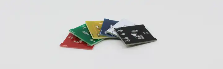
8. What color is the circuit board?
It seems that the color of the PCB is determined by the base material, but it is actually the solder mask. The substrate is usually green, but the solder mask above it can be blue, yellow, orange, purple, red, black, white, and of course green.
9. Does the color of the PCB matter?
There are many reasons to choose one, such as a specific color for the PCB substrate - whether it is a brand name, or if the boards in the system are pre-produced in one color and the boards can be produced in another color. Also, some colors are easier to see in contrast than with the naked eye, which can be an advantage when inspecting boards.
However, if lighting is to be used, choosing a white surface for the PCB can help reflect light. In some cases, this additional control provides more LED choices to optimize the design.
Depending on the application, reflected light may sometimes be required. In these applications, a white PCB is ideal.
White PCBs are usually used in LED light engines or LED lighting systems.
On the other hand, there may be applications where light reflections are undesirable, such as DJ equipment used in dark nightclubs.
The color of the substrate is only one of the factors to be considered in the schematic stage of PCB design.
10. What is the PCB design process like?
There are eight processes in the manufacture of printed circuit boards, the complexity of which can vary due to the design of the equipment:
PCB design basics (simple list)
1. The concept of electronic equipment
2. Electronic schematic diagram creation
3. Printed circuit board layout design
4. Final Bill of Materials (BOM)
5. Make PCB prototype
6. Evaluate the prototype
7. Install firmware/programming
8. Full production
The production process consists of the following steps:
1. Printed Circuit Board Design
2. Print the inner layer of copper
3. Remove excess copper
4. Check and Layer Alignment
5. Laminate layers
6. Drilling
7. PCB plating
8. RoHS Compliant
11. How long does it take to design and produce a custom PCB?
Turnaround time for custom PCBs depends on the supplier selected, as well as the complexity and volume of the project.
Like our PCB functions start from the design, to the end of the final completion, we are able to deliver turnaround service in as little as four weeks.
Dedicated warehouse space and advanced tools such as 3D printers allow our team to deliver rapid prototyping and speed up the process.
PCB
PCBA programming
pcb design
Agreed 14
Tim


Just upload Gerber files, BOM files and design files, and the KINGFORD team will provide a complete quotation within 24h.