
Professional PCB manufacturing and assembly
Building 6, Zone 3, Yuekang Road,Bao'an District, Shenzhen, China
+86-13410863085Mon.-Sat.08:00-20:00

When the signal line must leave the present pair of wiring layers to other wiring layers through the hole, the ground hole should be placed near the hole, so that the loop signal can be smoothly returned to the appropriate grounding layer. For layers 4 and 7, the signal loop will return from the power layer or ground layer (i.e., layer 5 or 6) because the capacitive coupling between the power layer and ground layer is good and the signal is easily transmitted.
If two power layers of the same voltage source need to output high current, the circuit board should be distributed into two groups of power layers and grounding layers. In this case, an insulating layer is placed between each pair of power layer and ground layer. This gives us the desired two pairs of power busbars with equal impedances for equal currents. If the stack of power layers results in unequal impedance, the shunt will be uneven, the transient voltage will be much larger, and EMI will increase dramatically.
If there are multiple power supply voltages with different values on the circuit board, multiple power layers are required accordingly. Remember to create separate power layers and connections for each power supply. In both cases, keep in mind the manufacturer's requirements for balanced structure when determining the position of the paired power layer and ground layer on the board.
summarize
Given that most of the circuit boards designed by engineers are traditional printed circuit boards with a thickness of 62mil and no blind or buried holes, the discussion of layering and stacking of circuit boards is limited here. The layered scheme recommended in this paper may not be ideal for boards with large thickness differences. In addition, the fabrication process of circuit boards with blind holes or buried holes is different, so the layering method in this paper is not applicable.
In circuit board design, the thickness, through hole process and the number of layers of circuit board are not the key to solve the problem. Good layered stacking is the key to ensure the bypass and decoupling of the power busbar, to minimize the transient voltage on the power layer or ground, and to shield the electromagnetic field of the signal and power. Ideally, there should be an insulating layer between the signal routing layer and the loop grounding layer, and the spacing of the paired layers (or more than one pair) should be as small as possible. According to these basic concepts and principles, the circuit board can always be designed to meet the design requirements. Now that the rise time of IC is already short and will be shorter, the techniques discussed in this article are essential to solving EMI shielding problems.
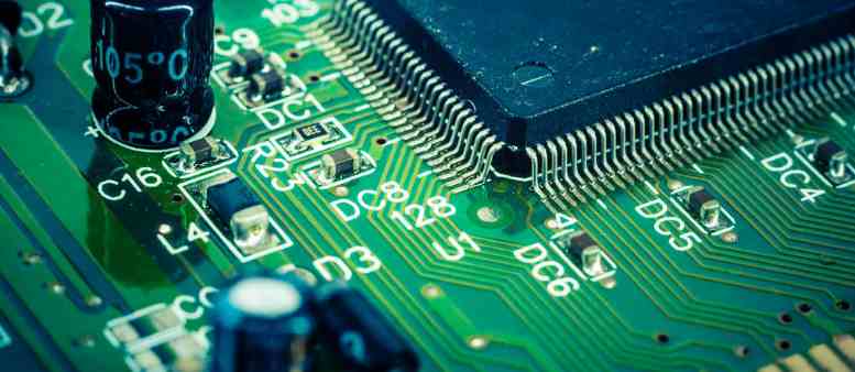
The basic principle of DC power supply design in high speed PCB design
Basic principles of DC power supply design in High speed PCB design:
1. The layout should meet the following requirements as far as possible:
The total connection should be as short as possible, the key signal line should be the shortest, the high-voltage and high-current signal should be separated from the small current, the low-voltage weak signal should be separated, the analog signal and the digital signal should be separated, the high-frequency signal and the low-frequency signal should be separated, and the interval of the high-frequency components should be sufficient.

For DC-DC power supply, the most important part includes: input and output capacitance, inductance, MOSFET, in Layout, these devices should be placed as close to the IC as possible, the smaller the loop, the better, do not arrange other circuits between the devices.
Power part and control part separate layout, power circuit is generally large voltage, large current, high power circuit, relatively large interference. And the control circuit is low voltage, if the control part to the power part, the control part is very likely to be disturbed, especially the power module in the single-side layout.
The wiring should be as short and thick as possible, and the copper skin should be laid as far as possible if it can break copper, because copper skin can improve the heat dissipation condition of the conversion device. Meanwhile, the non-moving point copper skin can capture the radio frequency energy and consume it well through eddy current to reduce the interference of Dianchi Lake.
2, power processing:
(1) The power ground and the control ground should be processed separately, and the grounding pin of the filter capacitor should be connected at a single point.
(2) Digital land and analog land should be separated, if the two types of land directly connected together, in some cases will cause serious consequences.
(3) Because there are coupled capacitors and distributed capacitors, there will be the same AC potential between the capacitors and the ground, so the power planes will also be separated.
(4) Digital ground and analog ground planes need to be separated and not overlapped. If overlapped, digital high-speed noise will be coupled to analog plane through distributed capacitance.
PCB design is extremely important
May 14,2023


Just upload Gerber files, BOM files and design files, and the KINGFORD team will provide a complete quotation within 24h.