
Professional PCB manufacturing and assembly
Building 6, Zone 3, Yuekang Road,Bao'an District, Shenzhen, China
+86-13410863085Mon.-Sat.08:00-20:00


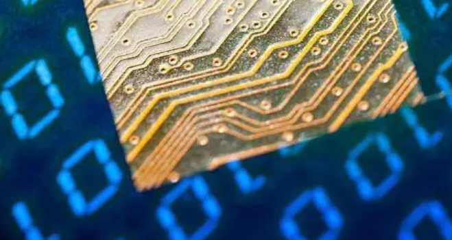
This paper mainly focuses on the concept and design principle of microwave high frequency circuit and PCB design, a frontier category of communication products. The PCB design principle of microwave-grade high frequency circuit is chosen because it has extensive guiding significance and belongs to the current hot application technology of high technology. The transition from microwave circuit PCB design concept to high-speed wireless network (including all kinds of access network) engineering is also in the same thread, because they are based on the same basic principle - dual transmission line theory.
Experienced RF engineers design digital circuits or relatively low frequency circuit PCB, the success rate is very high, because their design concept is based on the "distributed" parameter as the core, and the distributed parameter concept in lower frequency circuits (including digital circuits) the destructive effect is often ignored.
For a long time, many peers completed the design of electronic products (mainly for communication products), often fraught with problems. On the one hand, it is related to the lack of necessary elements in electrical design (including redundancy design, reliability design, etc.), but more importantly, many of these problems occur when people think that the necessary elements have been taken into account. To solve these problems, they often spend their energy on the verification of procedures, electrical principles, parameter redundancy and so on, but seldom spend their energy on the audit of PCB design, and it is often because of PCB design defects, leading to a large number of product performance problems.
PCB design principles involve many aspects, including the basic principles, anti-interference, electromagnetic compatibility, safety protection, and so on. For these aspects, especially in the high-frequency circuit (especially in the microwave level high-frequency circuit), the lack of relevant ideas, often leads to the failure of the entire research and development project. Many people still stay on the basis of "connecting electrical principles with conductors to play a predetermined role", and even think that "PCB design belongs to the scope of structural, technological and production efficiency considerations." Many professional RF engineers do not fully realize that this link should be the special focus of the whole design work in RF design, and mistakenly spend their energy on the selection of high-performance components, resulting in a large increase in cost, but little improvement in performance.

It is especially mentioned here that the digital circuit relies on its strong anti-interference, error detection and correction, and can be arbitrarily constructed various intelligent links to ensure the normal function of the circuit. A common digital application circuit with high add-on configuration of various "ensure normal" elements is clearly a product-free initiative. But often in the "not worth it" link, but lead to a series of product problems. The reason is that such functional links, which are not worth constructing reliability assurance from the perspective of product engineering, should be built on the working mechanism of digital circuit itself, but the wrong construction in circuit design (including PCB design) leads to an unstable state of the circuit. The cause of this unstable state belongs to the basic application of the same concept as the similar problem of high frequency circuits.
2. Layout of power cord
In general, in addition to interference caused directly by electromagnetic radiation, electromagnetic interference caused by power lines is the most common. Therefore, the layout of the power cable is also important, and the following rules should be followed in general.
(1) The power line should be as close as possible to the ground wire to reduce the area of the power supply loop, and the differential mode radiation is small, which is helpful to reduce the circuit interference. The power supply loops of different power supplies do not overlap each other.
(2) When adopting multi-layer process, analog power supply and digital power supply are separated to avoid mutual interference. Do not overlap the digital power supply with the analog power supply, or it will create coupling capacitance, breaking the degree of separation.
(3) Complete dielectric isolation can be used between the power plane and the ground plane. When the frequency and speed are very high, medium slurry with low dielectric constant should be selected. The power plane should be close to and below the ground plane to shield the radiation current distributed on the power plane.
(4) The power supply pin and ground pin of the chip should be decoupled. The decoupling capacitor is 0.01uF chip capacitor, which should be installed close to the chip to reduce the loop area of the decoupling capacitor as much as possible.
(5) When choosing the chip chip, try to choose the chip with the power pin close to the ground pin, which can further reduce the power supply loop area of the decoupling capacitor, and is conducive to the realization of electromagnetic compatibility.
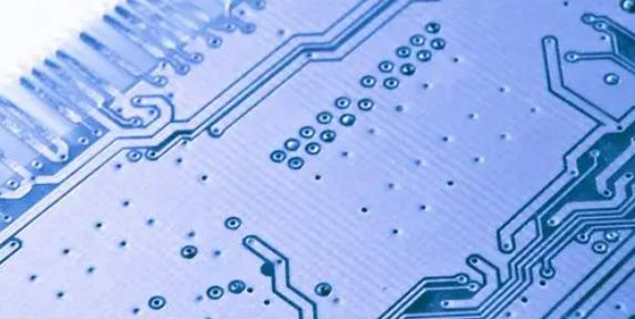
3. Layout of signal lines
When using the single-layer film process, a simple and applicable method is to first lay the ground wire, then place key signals such as high speed clock signals or sensitive circuits near their ground loops, and finally route other circuits. The layout of the signal line is best arranged according to the flow order of the signal, so that the signal on the circuit board is smooth.


Just upload Gerber files, BOM files and design files, and the KINGFORD team will provide a complete quotation within 24h.