
Professional PCB manufacturing and assembly
Building 6, Zone 3, Yuekang Road,Bao'an District, Shenzhen, China
+86-13410863085Mon.-Sat.08:00-20:00

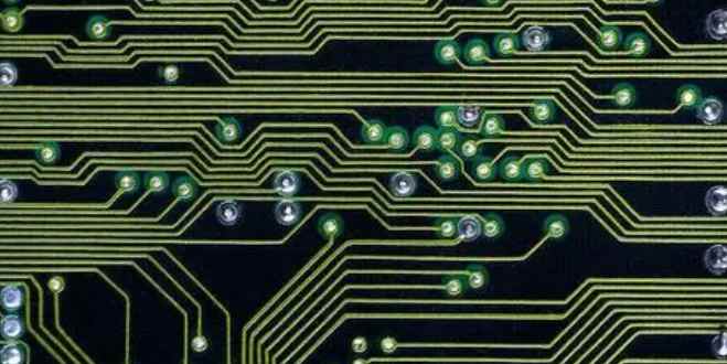
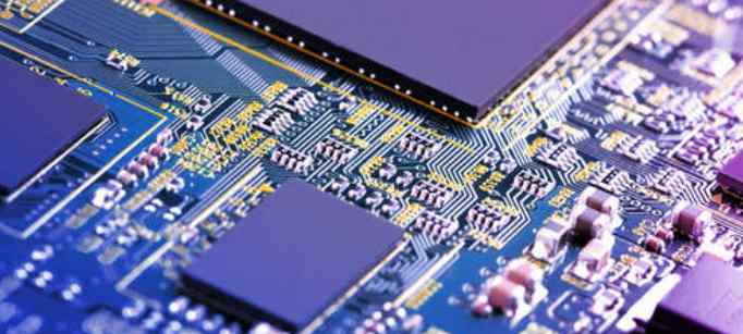
PCBS are almost identical on the outside, regardless of their inner quality. It is beneath the surface that we see the differences that are critical to the durability and function of PCBS throughout their life.
Whether in the manufacturing and assembly process or in actual use, PCB to have reliable performance, this is very important. In addition to the associated costs, defects in the assembly process may be carried by the PCB into the final product, which may break down during actual use, leading to claims. Therefore, from this point of view, it is safe to say that the cost of a good quality PCB is negligible.
In all market segments, especially those producing products in critical application areas, the consequences of such failures are dire.
These aspects should be kept in mind when comparing PCB prices. Although reliable, guaranteed and long-life products have higher initial costs, they are worth it in the long run.
The 14 most important characteristics of a highly reliable circuit board

1, 25 micron hole wall copper thickness
Benefits: Enhanced reliability, including improved Z-axis expansion resistance.
Risks of not doing so: blowing or degassing, electrical connectivity problems during assembly (inner separation, hole wall breakage), or the possibility of failure under load conditions in actual use. IPCClass2 (the standard adopted by most factories) requires 20% less copper plating.
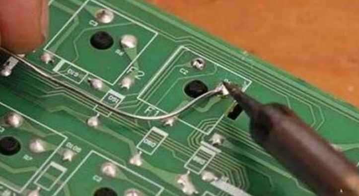
2. No welding repair or line repair
Benefits: Perfect circuit ensures reliability and safety, no maintenance, no risk
Risk of not doing this: If not repaired properly, the circuit board will be disconnected. Even if the repair is' properly ', there is a risk of failure under load conditions (vibration, etc.) which may occur in actual use.
3. Exceed the cleanliness requirements of IPC specifications
Benefits: Increased PCB cleanliness improves reliability.
Risks of not doing this: Residue and solder buildup on the circuit board pose risks to the solder shield, and ionic residue poses risks of corrosion and contamination of the weld surface, which can lead to reliability issues (poor solder joints/electrical failures) and ultimately increase the probability of actual failure.
4, strictly control the service life of each kind of surface treatment
Benefits: Solderability, reliability, and reduced risk of moisture intrusion
Risks of not doing so: Solderability problems can occur due to metallography changes in the surface treatment of older boards, and moisture intrusion can lead to delamination, inner layer and hole wall separation (break off) problems during assembly and/or actual use.
5. Use internationally known substrates -- no "local" or unknown brands
Benefits: Improved reliability and known performance
Risks of not doing this: Poor mechanical properties mean that the board will not perform as expected under assembled conditions. For example, high expansion properties can lead to delamination, circuit breaking, and warping problems. Weakening of electrical characteristics can result in poor impedance performance.
6. Copper clad plate tolerance meets the requirements of IPC4101ClassB/L
Advantage: Strict control of dielectric layer thickness can reduce the deviation of expected value of electrical performance.
Risks of not doing so: Electrical performance may not be up to the specified requirements, and the output/performance of the same batch of components may vary greatly.
7. Define solder resistance materials to ensure compliance with IPC-SM-840ClassT requirements
Benefits: NCAB Group recognizes "excellent" inks for ink safety and ensures that the solder resistance layer inks meet UL standards.
Risks of not doing so: Poor quality ink can lead to adhesion, flux resistance and hardness problems. All of these problems can cause the solder shield to detach from the circuit board and eventually lead to corrosion of the copper circuit. Poor insulation characteristics can cause short circuits due to unexpected electrical connectivity/arcing.
8. Define tolerances for shapes, holes and other mechanical features
Benefits: Strict tolerance control can improve the dimensional quality of the product - improve fit, shape and function
Risks of not doing this: Problems during assembly, such as alignment/fit (problems with pressing the mating pins are only discovered when the assembly is complete). In addition, loading the base can be problematic due to the increased size deviation.
9. NCAB specifies the solder shield thickness, although IPC does not specify it
Benefits: Improved electrical insulation, reduced risk of flaking or loss of adhesion, enhanced resistance to mechanical impact wherever it occurs!
Risks of not doing so: A thin solder shield can cause problems with adhesion, flux resistance and hardness. All of these problems can cause the solder shield to detach from the circuit board and eventually lead to corrosion of the copper circuit. Poor insulation due to thin solder resistance layer can cause short circuit due to unexpected conduction/arc.
10. Appearance requirements and repair requirements are defined, although IPC does not
Benefits: In the manufacturing process of careful care and careful casting safety.
Risks of not doing this: multiple scrapes, minor damage, patching and repairing - boards that work but don't look good. In addition to the visible problems, what are the hidden risks, the impact on assembly, and the risks in actual use?


Just upload Gerber files, BOM files and design files, and the KINGFORD team will provide a complete quotation within 24h.