
Professional PCB manufacturing and assembly
Building 6, Zone 3, Yuekang Road,Bao'an District, Shenzhen, China
+86-13410863085Mon.-Sat.08:00-20:00


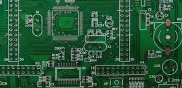
Let's first introduce the common drilling in PCB: through hole, blind hole, buried hole. The meaning and characteristics of these three holes.
Conduction hole (VIA), this is a common hole used to conduct or connect copper foil lines between conductive patterns in different layers of the circuit board. For example (e.g. blind holes, buried holes), but do not insert component pins or other reinforcement copper plated holes. Because PCB is formed by the accumulation of many copper foil layers, each layer of copper foil will be covered with a layer of insulation layer, so that the copper layer can not intercommunicate with each other, the signal link is on the through hole (via), so there is the Chinese through hole title.
Characteristics are: in order to meet customer needs, the circuit board through the hole must be strongholds, so in the change of the traditional aluminum sheet plug process, with white mesh to complete the circuit board surface welding and plug holes, so that its production stability, reliable quality, more perfect use. With the rapid development of the electronic industry, higher requirements have been put forward for the manufacturing process and surface mounting technology of printed circuit boards. The process of plugging through holes is applied and born, and the following requirements should be met: 1. Copper can be in the through hole, welding can plug or not plug. 2. There must be tin lead through the hole, there is a certain thickness requirement (4um) shall not be solder resistance ink into the hole, resulting in tin beads inside the hole. 3. The pass-through hole must have solder resistance ink plug hole, light proof, no tin ring, tin beads and flat requirements.

Blind hole: that is, the outermost circuit in the PCB and the adjacent inner layer to connect with electroplating holes, because can not see the opposite side, so called blind pass. At the same time, in order to increase the utilization of space between PCB layers, blind holes are applied. That is, a pass hole to a surface of the printed board.
Characteristics: Blind holes are located on the top and bottom surfaces of the board and have a certain depth. They are used to connect the surface circuit to the inner circuit below. The depth of the holes usually does not exceed a certain ratio (aperture). This production method needs to pay special attention to the depth of drilling (Z axis) to be just right, do not pay attention to it will cause difficulties in the hole electroplating so almost no factory, you can also put the prior need to connect the circuit layer in the individual circuit layer when the first drilling hole, and then together, but the need for more precise positioning and alignment device.
Buried hole is the link between any circuit layers inside the PCB, but not through to the outer layer, is also not extended to the surface of the circuit board of the through hole meaning.
Features: This process cannot be achieved by drilling after bonding. Drilling must be performed at the time of individual circuit layers. The inner layer must be partially bonded before electroplating treatment, and finally, all bonding can be completed. This process is usually used only on high-density circuit boards to increase the available space of other circuit layers
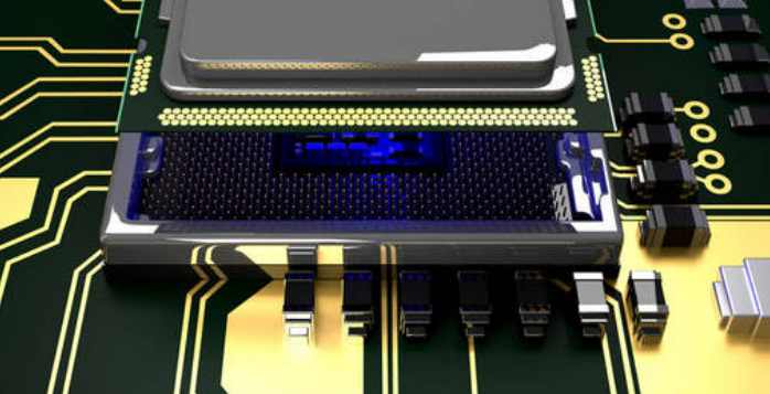
In PCB production process, drilling is very important, can not be careless. Because drilling is to drill the required holes in the copper clad plate, to provide electrical connection, fixing device function. If the operation is not proper, there is a problem in the process of the hole, the device can not be fixed on the circuit board, light will affect the use of heavy, the whole board will be scrapped, so the drilling process is very important.
11. Requirements for the depth of the plug hole
Benefits: High quality plugs will reduce the risk of failure during assembly.
The risk of not doing so
The chemical residue in the gold settling process can be left in the hole where the plug hole is not sufficient, causing problems such as weldability. Moreover, tin beads may be hidden in the hole, which may splash out during assembly or actual use, causing a short circuit.
12. PetersSD2955 specifies the brand and model of peelable blue glue
Benefits: The designation of peelable blue glue avoids the use of "local" or cheap brands.
The risk of not doing so
Poor quality or cheap peelable glue may bubble, melt, crack, or set like concrete during assembly, making the peelable glue unpeeled/ineffective.
13. NCAB implements specific approval and placing procedures for each purchase order
Benefit: This procedure is performed to ensure that all specifications have been confirmed.
The risk of not doing so
If product specifications are not carefully confirmed, the resulting deviations may not be discovered until assembly or the final product, when it is too late.
14. Sleeve plate with scrap unit is not accepted
Benefits: Not using partial assembly helps customers improve efficiency.
The risk of not doing so
Defective sheeting requires special assembly procedures. If the end-of-life unit board (x-out) is not clearly marked, or it is not isolated from the sheeting, the known defective board may be assembled, wasting parts and time.


Just upload Gerber files, BOM files and design files, and the KINGFORD team will provide a complete quotation within 24h.