
Professional PCB manufacturing and assembly
Building 6, Zone 3, Yuekang Road,Bao'an District, Shenzhen, China
+86-13410863085Mon.-Sat.08:00-20:00

PCB design refers to the production of circuit boards at the lowest possible cost through the design of schematic drawings and circuit layout. In the past, this was usually done with the help of expensive specialized tools, but now, with the increasing availability of free high-performance software tools and design models, the speed of design for board designers is greatly increased.
Although engineers know that a perfect design is the best way to avoid problems, it is a waste of time and money, while treating the symptoms rather than the root causes. For example, if a problem is discovered during electromagnetic compatibility (EMC) testing, it can cost a lot of money and even require tweaking and reworking the original design, which can take months.

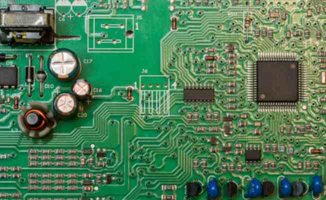
Layout is one of the first problems that designers face. Depending on the part of the drawing, some devices need to be set up together for logical reasons. It should be noted, however, that temperature-sensitive components, such as sensors, should be set up separately from heat-generating components, including power converters. For designs with multiple power Settings, 12-volt and 15-volt power converters can be located on different parts of the board because the heat and electronic noise they generate can affect the reliability and performance of other components and the board.
These components will also have an impact on the electromagnetic performance of circuit design, which is not only very important for the performance and energy consumption of the circuit board, but also for the economy of the circuit board. Therefore, all circuit board equipment sold in Europe must obtain the CE mark to prove that it will not cause interference to other systems. However, this is usually only in terms of power supply, and there are many devices that emit noise, such as DC-DC converters and high-speed data converters. Due to defects in circuit board design, these noises can be captured by the channel and radiated as small antennas, resulting in noise and frequency anomalies.
Far-field electromagnetic interference (EMI) problems can be solved by adding filters at noise points or by using metal casings to block signals. But the attention paid to the devices that emit electromagnetic interference (EMI) on the circuit board has made it possible to choose cheaper enclosures for the circuit board, thus effectively reducing the cost of the entire system.
In circuit board design process, electromagnetic interference (EMI) is indeed a factor that must be paid attention to. Electromagnetic crosstalk can be coupled with the channel, thus disrupting the signal into noise and affecting the overall performance of the circuit board. If the coupling noise is too high, the signal may be completely overridden, so a more expensive signal amplifier must be installed to restore normal. However, if at the beginning of the board design, can fully consider the layout of the signal line, these problems can be avoided. Because the design of the circuit board will vary according to different equipment, different use locations, different heat dissipation requirements, and different electromagnetic interference (EMI) situation, then the design template is in great use.
Capacitance is also an important issue in circuit board design, because it can affect the propagation speed of signals and increase the consumption of electricity. A channel can inadvertently form a capacitor by coupling to a nearby line or crossing two layers vertically. These problems can be solved relatively easily by reducing the length of parallel lines and by adding kinks to one of the lines to break the coupling. However, this also requires the engineer to fully consider production design principles to ensure that the design is easy to manufacture while avoiding any noise radiation caused by excessive line bending angles. The lines can also be too close together, which can create short loops between the lines, especially where the lines are bent, and metal "whiskers" can appear over time. Design rule checks can often flag areas where the loop is riskier than normal.
This problem is particularly prominent in the design of the stratum. A layer of metal circuits that may be coupled to all the lines above and below it. Although the metal layer does effectively block noise, it also creates associated capacitance, which affects the speed of the line and increases power consumption.
As far as the design of multilayer circuit boards is concerned, the through-hole design between different circuit board layers is probably the most controversial one, because the through-hole design will bring many problems to the manufacture of circuit boards. The through hole between the circuit board layer will affect the performance of the signal and reduce the reliability of the circuit board design, so it should be paid full attention to.
Rf circuit PCB design
Mar 30,2023


Just upload Gerber files, BOM files and design files, and the KINGFORD team will provide a complete quotation within 24h.