
Professional PCB manufacturing and assembly
Building 6, Zone 3, Yuekang Road,Bao'an District, Shenzhen, China
+86-13410863085Mon.-Sat.08:00-20:00

(I) Introduction
The development and change of electronic technology will inevitably bring many new problems and challenges to board design. First of all, due to the high density of pins and the increasing physical limit of pin size, resulting in low spread rate; Secondly, due to the increase of the system clock frequency, the timing and signal integrity problems; Third, engineers want better tools for complex, high-performance designs on the PC platform. Therefore, it is not difficult to see that PCB board design has the following three trends:
The design of high speed digital circuits (i.e. high clock frequency and fast edge rate) became mainstream.
Product miniaturization and high performance must face the problem of distribution effect caused by mixed-signal design technology (i.e. digital, analog and RF hybrid design) on the same PCB board.
The increase of design difficulty leads to the traditional design process and design methods, as well as CAD tools on PC are difficult to meet the current technical challenges, therefore, EDA software tool platform from UNIX to NT platform has become a trend recognized in the industry.
(2) High frequency circuit wiring skills
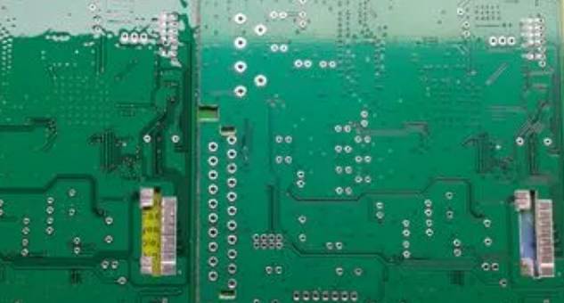
High frequency circuits often have high integration and high wiring density. The use of multilayer is not only necessary for wiring, but also an effective means to reduce interference.
High frequency device pins require as little lead bending as possible. It is best to use the lead of high frequency circuit wiring fully straight line, need to turn, can be used 45° broken line or arc turn, this requirement in low frequency circuit is only used to improve the copper foil fixation strength, and in high frequency circuit, meet this requirement can reduce the high frequency signal to the external emission and mutual coupling.
The shorter the lead of the pin of the high frequency circuit device, the better.
The frequency circuit device pin to ask the lead layer to alternate as little as possible. The fewer holes (Via) used during component connection, the better. It has been measured that one hole can bring about 0.5pF of distributed capacitance, and reducing the number of holes can significantly increase the speed.
For high frequency circuit wiring, attention should be paid to the crosstalk introduced by short distance parallel routing of signal lines. If parallel distribution cannot be avoided, a large area can be arranged on the opposite side of parallel signal lines to greatly reduce interference. It is almost impossible to avoid parallel lines within the same floor, but the direction of the two adjacent floors must be perpendicular to each other.
Especially important signal lines or local units to implement ground encircling measures.
All signal cables cannot be routed in a loop, and ground cables cannot be routed in a current loop.
At least one high-frequency decoupling capacitor should be located near each integrated circuit block (IC), and the decoupling capacitor should be as close to the Vcc of the device as possible.

Analog ground wire (AGND), the digital ground (DGND), such as high frequency should be used when the public earthed choke this link. In the actual assembly of high frequency choke links, high frequency ferrite magnetic beads with wires through the center are often used, which can be regarded as inductors in the schematic diagram. A component package is defined separately for it in the PCB component library, and it is manually moved to a suitable position near the convergence of the common ground wire before wiring.
(3) Design method of electromagnetic compatibility (EMC) in PCB
PCB substrate selection and PCB layer setting, electronic component selection and electromagnetic characteristics of electronic components, component layout, component interconnect length and width are restricted to PCB electromagnetic compatibility. The integrated circuit chip (IC) on PCB is the main energy source of electromagnetic interference (EMI). Conventional electromagnetic interference (EMI) control technologies generally include: reasonable layout of components, reasonable control of wiring, power line, grounding, reasonable configuration of filter capacitance, shielding and other measures to inhibit electromagnetic interference (EMI) are very effective, and are widely used in engineering practice.
1. Wiring rules for Electromagnetic Compatibility (EMC) design of high frequency digital Circuit PCB
High frequency digital signal cables should be short, generally smaller than 2inch(5cm), and the shorter the better.
The main signal line is best concentrated in the center of the PCB board.
The clock generator circuit should be near the center of the PCB board, and the clock fan out should be Daisy chain or parallel wiring.
Power lines should be kept as far away from high frequency digital signal lines or ground lines as possible, and the distribution of power must be low induction (multiplex design). The power layer in the multilayer PCB board is adjacent to the ground, which is equivalent to a capacitor and plays the role of filtering. Power cables and ground cables on the same floor should be as close as possible. The copper foil around the power layer should be indented 20 times the size of the distance between the two flat layers to ensure better EMC performance of the system. Do not divide the ground plane. If the high-speed signal line is to be divided across the power plane, several low-impedance bridging capacitors should be placed close to the signal line.
Input and output wires should be as close to each other as possible. It is better to add ground wire to avoid feedback coupling.
When the thickness of copper foil is 50um and the width is 1-1.5mm, the current through 2A, the conductor temperature < 3 ° C. PCB board wires should be wide as far as possible. For integrated circuits, especially for signal wires of digital circuits, the wire width of 4mil-12mil is usually used, and the wire width of power cables and ground wires should be greater than 40mil. The minimum wire spacing is mainly determined by the insulation resistance and breakdown voltage between the wires in the worst case, and the wire spacing above 4mil is usually chosen. In order to reduce the cross talk between wires, the distance between wires can be increased if necessary, and the ground wire can be installed as the isolation between wires.
Signal integrity and design of PCBS
Mar 30,2023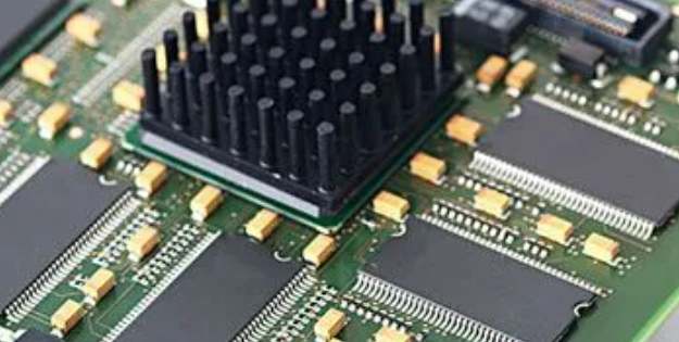


Just upload Gerber files, BOM files and design files, and the KINGFORD team will provide a complete quotation within 24h.