
Professional PCB manufacturing and assembly
Building 6, Zone 3, Yuekang Road,Bao'an District, Shenzhen, China
+86-13410863085Mon.-Sat.08:00-20:00

When hardware engineers first came into contact with multilayer PCBS, they involved common multilayer and HDI PCB boards. Now they use stereo graphics to show the internal architecture of pcb drawings of various laminated structures. Isn't that straightforward?
Multi-layer PCB line processing, and single layer and double layer no difference, the biggest difference in the hole process.
Lines are etched out, holes are drilled and then copper plated out, these do hardware development we all understand, do not repeat.
Multilayer circuit board, usually through the hole plate, first board, second board, second stack plate these several. Higher level such as the third level board, arbitrary layer interconnection board usually used very little, the price thief expensive, not to discuss.
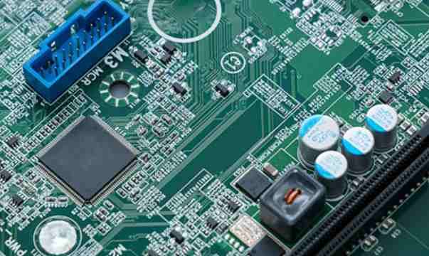
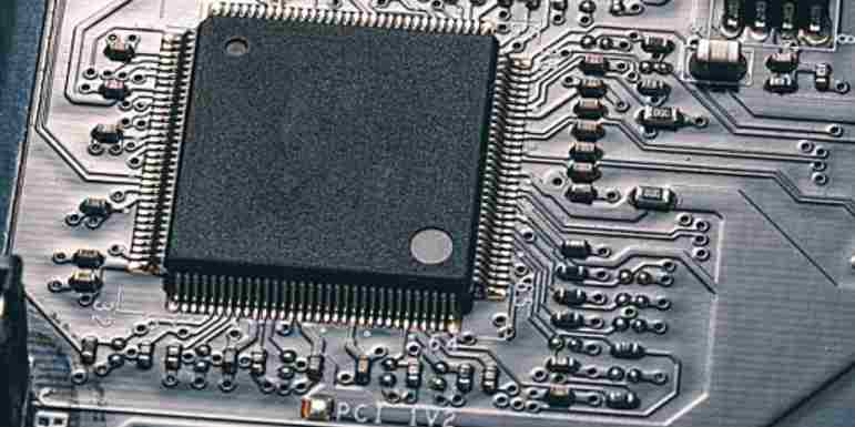
Under normal circumstances, 8-bit single-chip microcomputer products with 2 layers of through hole plate; 32-bit single-chip level intelligent hardware, using 4-6 layers of through hole plate; Linux and Android level smart hardware, using 6-layer through hole to 8-layer first-stage HDI board;
Smart phone such compact products, generally use 8 layers of the first level to 10 layers of the second level circuit board.
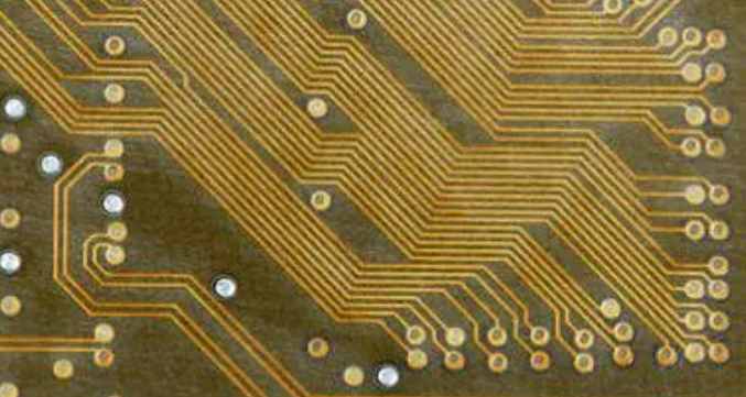
Our most common through hole. There is only one perforation, from the first layer to the last layer. No matter the external line or the internal line, the hole is pierced. It's called a through-hole plate.
Through the hole plate and the number of layers does not matter, usually we use 2 layers are through the hole plate, and many switches and military circuit boards, do 20 layers, or through the hole. The circuit board is drilled through with a drill and copper plated in the holes to create a path.
Note that the inner diameter of the through hole is usually 0.2mm, 0.25mm and 0.3mm, but generally 0.2mm is much more expensive than 0.3mm. Because the drill bit is too thin and easy to break, the drill is also slow. The extra time and drill costs are reflected in the rising price of circuit boards.
Laser hole of the lower high density board (HDI board)
This is a 6 - layer 2 - order staggered HDI board. Usually we use 6 layers of 2 less, most of the 8 layers of 2. There are more layers here, same thing as six layers
The so-called second order, there are two layers of laser holes.
The so-called wrong hole, is the two layers of laser holes are staggered.
Why stagger it? Because the copper plating is not satisfied, the hole inside is empty, so it can not be directly punched on the above, to stagger a certain distance, and then hit a layer of empty.
Six levels of second order is equal to four levels of first order plus two levels.
Eight levels of second order is equal to six levels of first order plus two levels.
Laminated plate, the process is complex and the price is higher

The two layers of laser holes in the staggered plate overlap each other, making the line more compact.
The inner laser hole needs to be electroplated and filled, and then the outer laser hole is made. The price is more expensive than the error hole.
Super expensive arbitrary layer interconnect board, multi-layer laser hole stack
Each layer is a laser hole, and each layer can be connected together. Line the line however you want, punch the hole however you want.
Layout engineers think about it! No longer afraid not to draw!
Purchasing just think about crying, more than 10 times more expensive than the ordinary through hole plate!
So, only products like the iPhone are willing to use. Other phone brands, no one has ever heard of using any layer interconnection board.
Let's finish with a picture and compare it more closely.
Note the size of the hole and whether the pad for the hole is closed or open
FPCB materials and procedures make the terminal flexible performance improved
FPCBS are used in many products, but basically nothing more than lead circuit, printed circuit, connector and multifunctional integration system. According to the function, it can be divided into space design, change its shape, folding, bending design group, and FPCB design can be used to prevent the static interference of electronic equipment. And the use of soft circuit board, if the cost, let the quality of production directly on the soft board architecture, not only the design volume is relatively reduced, the volume of the overall product can also be greatly reduced because of the characteristics of the board.
FPCB substrate structure is quite simple, mainly by the upper protective layer, the middle of the wire layer, in mass production soft particle path plate can be matched with positioning holes for production program alignment and post-processing. As for the use of FPCB, according to the space needs to change the shape of the board, or use the folding form, and multi-layer structure as long as in the outer EMI, electrostatic barrier design form, soft circuit board can also achieve efficient EMI problems to improve the design.
On the key circuit board, the topmost structure of FPCB is Copper, which can be divided into RA (Rolled Annealed Copper) and ED (Electro Deposited copper). The manufacturing cost of ED copper is quite low, but the material is easy to be rolled or faulted. RA (Rolled Annealed Copper) has high production cost, but its softness performance is good. Therefore, RA materials are mostly applied in flexible circuit boards in high flexural conditions.
As for FPCB to form, the Adhesive coating, calendered copper and substrate need to be bonded through adhesive. The commonly used adhesive include Acrylic and Mo Epoxy, which have low thermal resistance and are mainly used by domestic products. And acrylic although high heat resistance, high strength, but its electrical insulation is poor, and in the FPCB production structure, the thickness of the following agent accounted for the overall thickness of 20~40μm (micron).


Just upload Gerber files, BOM files and design files, and the KINGFORD team will provide a complete quotation within 24h.