
Professional PCB manufacturing and assembly
Building 6, Zone 3, Yuekang Road,Bao'an District, Shenzhen, China
+86-13410863085Mon.-Sat.08:00-20:00

With the development of science and technology, many electronic products are developing in the direction of small and fine, so that the size of many patch components is getting smaller and smaller, not only the requirements of the processing environment are constantly improving, but also the SMT processing technology has higher requirements. In order to do a good job of PCBA processing, SMT patch factory needs to do at least the following three points.
First, when SMT processing is carried out, we all know that solder paste is needed. For the solder paste just bought, if it is not used immediately, it must be placed in the environment of 5-10 degrees for storage, in order not to affect the use of the solder paste, must not be able to be placed in the environment below zero.
Second, when SMT process is mounting, the equipment of the SMT machine must be checked frequently. If the equipment is aging or some zero components are damaged, the equipment must be repaired or replaced with new equipment in order to ensure that the patch will not be slanted and high material throwing occurs. Only in this way can we reduce production costs and improve production efficiency.
Thirdly, when SMT processing is carried out, if the welding quality of PCB board is to be guaranteed, it is necessary to always pay attention to whether the setting of reflow welding process parameters is very reasonable. If the parameter setting is wrong, the welding quality of PCB board cannot be guaranteed. Therefore, under normal circumstances, the furnace temperature must be tested twice a day, and the minimum must be tested once. Only by constantly improving the temperature curve and setting the temperature curve of welding products, can we ensure the quality of processed products.

2.PCBA processing upright Micro-USB connector pin short circuit and air welding problem sharing
When the new product was being developed, the vertical micro-USB connector was not available on the market, so our institutional R&D engineers went directly to the connector manufacturer to develop and design a new micro-USB connector. This was the beginning of a manufacturing nightmare.
kingford is under the impression that as long as we find suppliers to cooperate with our products and develop our own connectors, there will be problems in the end. The previous 10P8C short-circuit problem is a tragic example, while this micro-USB connector has the dual problems of pin short-circuit and air welding.
kingford believes that parts that have not been extensively verified in the market, especially connectors, are prone to problems, because they do not necessarily know some small details of parts manufacturing and production when they are doing system research and development. They usually only pay attention to system functions, while ignoring some small details of parts design, and defects in small details may eventually develop into big problems.
At the beginning, when we were developing the connector, we used the pin terminal structure, because these pin terminals are needle-shaped copper products, which are easy to bend and shape, and can be bent into various shapes as required, and can also be made into L-shaped gull-wing pins, which are convenient for SMT patches to eat tin.
However, because the pin terminal is easy to bend, it is easy to cause problems such as pin deformation and poor coplanarity. Finally, the welding pin is not easy to stick to the circuit board, resulting in false welding, or in the process of transport, collision and short circuit of the solder.
In order to solve this problem, we actually made a lot of efforts, such as increasing the amount of solder in the local pin position to reduce the ratio of false welding, adding red glue and increasing the positioning column to reduce the ratio of pin offset short circuit, but the effect is not good, because the source (connector factory) quality is not good, how to follow-up efforts, the effect is only half the effort.
The PCBA foundry repeatedly gave feedback on the quality problem of the connector, and the PCBA foundry directly asked the connector manufacturer for compensation for loss, so the connector manufacturer finally put forward a constructive improvement plan. Pressure makes progress
The method of changing the terminal from "pin arrangement" to "metal stamping part" is very simple, that is, the terminal is directly shaped into the connector pin through the gold stamping process, so that the pin arrangement is not formed into the terminal and pin through the multi-channel bending procedure, which reduces the risk that the size is not easy to control in the multi-channel bending process. It also greatly reduces the risk of re-deformation due to bending stress after terminal forming, and the integrated metal structure is much stronger than the needle structure after multiple bending. In fact, this kind of stamping terminal design also often appears in the high-density flexible wire connector, and the application has been quite mature, but the manufacturing cost is relatively expensive, and a new gold mold is needed.
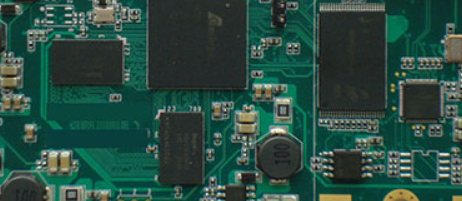
SMT patch processing capability
1. Maximum board card: 310mm*410mm(SMT);
2. Maximum plate thickness: 3mm;
3. Minimum plate thickness: 0.5mm;
4. Minimum Chip parts: 0201 package or parts above 0.6mm*0.3mm;
5. Maximum weight of mounted parts: 150g;
6. Maximum parts height: 25mm;
7. Maximum parts size: 150mm*150mm;
8. Minimum spacing of pin parts: 0.3mm;
9. Minimum ball parts (BGA) spacing: 0.3mm;
10. Minimum ball parts (BGA) ball diameter: 0.3mm;
11. Maximum parts mounting accuracy (100QFP) : 25um@IPC;
12. Patch capacity: 3-4 million points/day.
Why do you choose Shenzhen kingford for SMT processing?
1. Strength guarantee
▪SMT workshop: We have imported SMT machines and several sets of optical inspection equipment, with a daily output of 4 million. Each process is equipped with QC personnel, who can keep an eye on product quality.
▪DIP production line: We have two wave-soldering machines, among which there are more than 10 old employees who have worked for more than three years. The skilled workers can weld all kinds of plug-in materials.
2. Quality assurance, cost-effective
▪ High-end equipment can stick precision shaped parts, BGA, QFN, 0201 materials. Can also template patch, loose material hand.
▪ Sample and size batch can be produced, proofing from 800 yuan, batch 0.008 yuan/point, no start-up fee.
3. Rich experience in SMT and welding of electronic products, stable delivery
▪ Accumulated SMT SMT processingservices for thousands of electronic enterprises, involving many kinds of automotive equipment and industrial control motherboard. The products are often exported to Europe and the United States, and the quality can be affirmed by new and old customers.
▪ On time delivery, normal 3-5 days after complete materials, small batch can also be expedited on the same day shipment.


Just upload Gerber files, BOM files and design files, and the KINGFORD team will provide a complete quotation within 24h.