
Professional PCB manufacturing and assembly
Building 6, Zone 3, Yuekang Road,Bao'an District, Shenzhen, China
+86-13410863085Mon.-Sat.08:00-20:00

Quality inspection is the key link to ensure the quality of SMT patch factory. Only by strictly implementing the quality inspection procedure can the quality of electronic processing products meet the needs of customers. AOI occupies a crucial position in the production process of patch processing and makes a great contribution to the quality assurance. Next, Shenzhen SMT patch processing manufacturer - Shenzhen Honglijie will introduce the role of AOI in SMT patch processing in detail.
The role of AOI in SMT patch processing
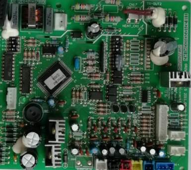
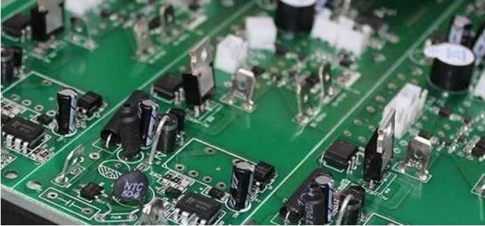
AOI (Automated Optical Inspection) is the Chinese full name of automatic optical inspection, is based on the optical principle to detect the common defects encountered in welding production equipment. AOI is a new type of testing technology, but the development is rapid, many manufacturers have launched AOI testing equipment. When automatic detection, the machine automatically scans PCB through the camera, collects images, compares the solder joints tested with qualified parameters in the database, checks the defects on the PCB through image processing, and displays/marks the defects through the display or automatic signs for repair personnel to repair. The high speed and high precision visual processing technology is used to automatically detect various mounting errors and welding defects on PCB board. PCB board can range from fine spacing high density board to low density large size board, and can provide online testing solutions to improve production efficiency, and welding quality. By using AOI as a defect reduction tool, errors are found and eliminated early in the assembly process to achieve good process control. Early detection of defects will avoid sending broken boards to the subsequent assembly stage, and AOI will reduce repair costs and avoid scrapping unrepairable boards.
AOI is actually an optical identification system, which has been widely used in today's electronic processing industry and has gradually replaced the traditional manual visual inspection method. Generally, image technology is used to judge whether the object to be measured meets the standard by comparing whether there is too much difference between the object to be measured and the standard image. In the actual SMT plant, AOI is used to test the processing quality of electronic components on the circuit board and whether the solder paste meets the processing standards, so that problems can be found in time and solved in advance.
In addition, it is widely used in pre-furnace and post-furnace testing. Before the furnace, it can confirm whether solder paste printing and component mounting meet the processing requirements, and timely correct the defective parts in the patch processing. After the furnace, AOI can timely detect some welding defects in the reflow welding process, and deal with them in time to avoid flowing into the next processing link. The biggest disadvantage of AOI in SMT patch processing is that there are some gray scale or shadow shading is not very obvious, which is easy to misjudge. These may be identified by using different colors of light, but the most troublesome is those components covered by other parts and the solder joints located under the components. Because traditional AOI can only detect where direct light can reach, such as the screen frame rib or the element under its edge, often because AOI can't detect the past.

2. Influence of PCB quality on PCBA processing
PCBA processing is a very complex process. The whole PCBA process seems to differ from PCB in one word. In fact, it changes a lot. PCBA has a range of PCB-based back-end processes such as solder paste printing, SPI testing, SMT processing, reflow soldering, DIP post soldering, wave soldering/selective wave soldering, PCBA first part testing, etc.
All processes of PCBA processing are based on PCB board, so the quality of PCB determines the quality of the whole PCBA. So what aspects of PCBS have an impact on PCBA?
First, PCB board surface dirty
Dirty board surface is mainly caused by high solid content of flux, large coating amount, preheating temperature is too high or too low, or the conveyor belt PCB clamp claw is too dirty, tin groove oxide and tin slag too much.
Solution: Choose the appropriate flux; Control flux coating amount; Control preheating temperature; Check the cleaning effect of automatic cleaning PCB gripper and take measures; Timely clean the oxide and tin slag on the surface of the tin tank.
Two, white slag
The white residue is often called white cream. Although does not affect the surface insulation resistance, but the customer does not accept.
Solution: first use flux and then use solvent cleaning; If it cannot be cleaned, it may be due to aging of the flux, exposure to the air to absorb water vapor, high moisture content in the cleaning agent (solvent), or a mismatch between the flux and the cleaning agent, and the supplier should be asked to help solve or replace the flux cleaning agent.
Three, PCB deformation
PCB deformation is mainly caused by excessive PCB quality or uneven component layout.
Solution: In the design of PCB, try to make the components distributed evenly. A support belt is designed in the middle of large-size PCB (the design width of non-layout component area is 2~3mm); Or use a mass balance tool to press sparse components on PCB in the welding process to achieve mass balance.
Shenzhenkingford PCBA processing capacity
1. Maximum board card: 310mm*410mm(SMT);
2. Maximum plate thickness: 3mm;
3. Minimum plate thickness: 0.5mm;
4. Minimum Chip parts: 0201 package or parts above 0.6mm*0.3mm;
5. Maximum weight of mounted parts: 150g;
6. Maximum parts height: 25mm;
7. Maximum parts size: 150mm*150mm;
8. Minimum spacing of pin parts: 0.3mm;
9. Minimum ball parts (BGA) spacing: 0.3mm;
10. Minimum ball parts (BGA) ball diameter: 0.3mm;
11. Maximum parts mounting accuracy (100QFP) : 25um@IPC;
12. Patch capacity: 3-4 million points/day.
Why choose Shenzhen kingford to do PCBA processing?
1. Strength guarantee
▪SMT workshop: We have imported SMT machines and several sets of optical inspection equipment, with a daily output of 4 million. Each process is equipped with QC personnel, who can keep an eye on product quality.
▪DIP production line: We have two wave-soldering machines, among which there are more than 10 old employees who have worked for more than three years. The skilled workers can weld all kinds of plug-in materials.
2. Quality assurance, cost-effective
▪ High-end equipment can stick precision shaped parts, BGA, QFN, 0201 materials. Can also template patch, loose material hand.
▪ Sample and size batch can be produced, proofing from 800 yuan, batch 0.008 yuan/point, no start-up fee.
3. Rich experience in SMT and welding of electronic products, stable delivery
▪ Accumulated SMT SMT processing services for thousands of electronic enterprises, involving many kinds of automotive equipment and industrial control motherboard. The products are often exported to Europe and the United States, and the quality can be affirmed by new and old customers.
▪ On time delivery, normal 3-5 days after complete materials, small batch can also be expedited on the same day shipment.
4. Strong maintenance ability and perfect after-sales service
▪ Experienced maintenance engineers can repair all kinds of patch welding caused by bad products, to ensure the connection rate of each piece of circuit board.
▪ 24-hour customer service staff at any time response, the fastest speed to solve your order problems.


Just upload Gerber files, BOM files and design files, and the KINGFORD team will provide a complete quotation within 24h.